2.5D & 3D ICs — Do We Have A Liftoff?
All the work that’s been done on stacked die really could pay off soon.
The challenges of Moore’s law scaling at advanced technology nodes are well documented. I won’t repeat them here. The benefits of “more than Moore” scaling (i.e., 2.5D and 3D ICs) are also well-known. This technology has shown great promise to provide an alternate path for large-scale integration. The technology has seen a lot of research effort, infrastructure support, standards development and technical publication. It’s just about ready to enter the mainstream, and it’s been this way for a while now. And that’s the problem.
I’ve personally been involved in 3D IC efforts for several years now. In the early days, my focus was on 3D IC “stack planning.” Translation: Tools to help understand which 2.5/3D IC stack configuration will provide the desired power, performance and cost profile. Questions addressed here include what type of memory and memory interface to use, what type of (and how many) interposers are required and which function to map to what technology node. Many options to consider, typically with budget to implement only one of them, so it better be the right one.

Much work was expended on building these tools, and the user base was quite small, but very smart and vocal. I would often get asked when all this work would pay off with higher tool sales. I would always say the same thing. “Soon, 2.5/3D IC is just about to take off.”
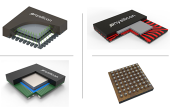
More recently, I’ve been looking at the problem from the implementation end of the spectrum. How to build substrates for 2.5D ICs and how to integrate the system on them. There are many challenges here. What substrate material, what routing pitch, how to source and test the die that go onto that substrate and so on. eSilicon presented some pioneering work at a recent 3D IC conference regarding a 2.5D system built with an organic substrate. The results are quite promising and we believe this technology will see significant interest, as 2.5/3D IC is just about to take off.
The good news is that this time, liftoff for 2.5/3D IC might be real. There is a definite increase in the number of product plans incorporating this technology. A basic driver for any new technology like this is cost. Test and yield drive cost, and there are promising improvements in both areas. New strategies to test at the die-level more efficiently are emerging. Process improvements are making silicon substrates more reliable, and organic substrates are showing great promise as well. Initial products will likely be based on 2.5D technology, with full (vertical stack) 3D implementation following later.
So, if you’re a substrate vendor, semi equipment supplier, EDA tool developer or IP developer, maintain a positive outlook. All that work could pay off soon…
__________________________________________
This is a guest post by Mike Gianfagna of eSilicon