

Category Archives: Wafer and Foundries
Semiconductor Sales Forecast 2019-2025

IC Insights’ August and September Updates to the 2021 McClean Report featured a two part analysis on the global IC foundry market. The total foundry market consists of pure-play foundries like TSMC, GlobalFoundries, UMC, and SMIC—companies that only produce ICs for other companies and integrated device manufacturer (IDM) foundries like Samsung and Intel that offer
Read MoreSemiconductor Wafer Capacity by Geographic Region (2020)

IC Insights’ Global Wafer Capacity 2021-2025 report breaks out the world’s installed monthly wafer capacity by geographic region (or country). Figure 1 shows the installed capacity by region as of December of 2020.
To clarify what the data represents, each regional number is the total installed monthly capacity of fabs located
Semiconductor Foundry
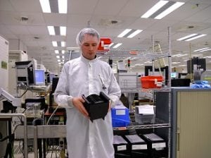
Figure 1: GlobalFoundries Fab1 in Dresden Germany
What is a Semiconductor Foundry?
In simple terms, a semiconductor foundry (also known as a fab) is a factory where silicon wafers are manufactured. The main customers of a semiconductor foundry are chip makers such as: Broadcom, Qualcomm, Intel, AMD and
Semiconductor Manufacturing Overview
When we say semiconductors, what is the first thing that comes to mind? Most of the time we think about computer chips and transistors, but it’s not as simple as it seems. For us to be able to get a basic understanding of the process of manufacturing semiconductors, we need
Read MoreFabless Suppliers Held a Record 33% of the 2020 IC Market

IC Insights’ April Update to the 2021 McClean Report describes how the sales growth rates of fabless IC companies versus IDM (integrated device manufacturers) IC suppliers have historically been very different (Figure 1). Typically, the sales growth rate registered by the fabless IC suppliers is better than that displayed by the IDMs. In
Read MoreFirst Google-Sponsored MPW Shuttle Launched at SkyWater with 40 Open Source Community Submitted Designs
BLOOMINGTON, Minn. and SAN JOSE, Calif. – April 6, 2021 – SkyWater Technology, the trusted technology realization partner, and Efabless, a crowdsourcing design platform for custom silicon, today announced the first tapeout in a series of Google-sponsored open source multi-project wafer (MPW) shuttles, managed by Efabless and manufactured at SkyWater. In this partnership, open
Read More