CDM ESD Testing: Getting a Clearer Picture
Of all of the component-level ESD tests available, the CDM ESD (charged-device model) test is the closest to simulating real world events. CDM ESD testing simulates ESD charging followed by a rapid discharge, similar to what is seen in the automated handling, manufacturing, and assembly of IC devices. Unfortunately, the CDM ESD test sometimes gives confusing results. Some examples include the following:
- Different results are seen when a part is stressed at different labs, even at the same voltage level.
- A part tested at +/-450V fails, but later passes at +/-500V.
- A part tested at +/-250V passes, but another sample of parts from the same lot fails at +/-250V.
EAG has investigated some of the more common causes of variability in the CDM test. Incorrect measurement of the current-versus-time waveform, which occurs during the discharge event, has been found to be the most important source of variation. Better measurement of the CDM waveform, using higher-bandwidth oscilloscopes to eliminate system-to-system variation, leads to more repeatable test results. This will become even more important in the near future when the ESDA and JEDEC release their joint CDM specification.
Overview of the JEDEC CDM ESD test
Figure 1, from JESD22-C101F, shows a generic CDM test circuit. It includes a discharge head with a pogo pin, a 1Ω radial resistor, the top ground plane, a semi-rigid coaxial cable, and the test head support arm. The test head is robotically driven, and it often has two small cameras that are used to align the test head in the correct position over the device under test (DUT). The potential of the DUT is raised by the field-induced method. A test voltage is applied to the field-charging electrode. The DUT sits in the “dead bug” (pin up or ball up configuration) on an FR-4 dielectric that covers the field-charging electrode. Once the DUT has been charged, the device is discharged by having the pogo pin touch each DUT pin, one at a time. At least one positive and one negative discharge is applied to every DUT pin. If the DUT no longer meets its data sheet specifications after the CDM stress, it is considered to be a failing unit.

Figure 1 – Generic CDM Circuit
The CDM tester is verified to be in spec by using a 1GHz/5Gigasamples/sec oscilloscope to measure the current-versus-time waveform when the DUT is one of the standard JEDEC capacitors. The specifications for the small and large disk capacitors are found in the JEDEC CDM specification, JESD22-C101F. The generic discharge waveform is shown in Figure 2.

Figure 2-CDM Discharge Waveform
To be in spec, the waveform must have characteristics that meet the requirements defined in Table 3 of the CDM specification.
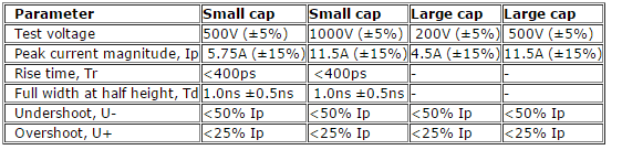
Table 3-CDM Waveform Characteristics
Common Sources of CDM Test Variability Can be Controlled or Characterized
In the CDM test, it is relatively easy to raise the field-charging electrode to the proper voltage. Unfortunately, the correct voltage on the charge plate is insufficient to guarantee a repeatable CDM event. Most of the variability in the CDM test comes from the discharge event. The sources of variability include the following:
- JEDEC test head differences
- Waveform measurement
- Charging time
- Size of ground plane
- Pogo pin variables (size, cleanliness, etc.)
- Capacitor disk
- 1Ω radial resistor
- Humidity control (<60%)
Most of these sources of variation can be characterized or controlled. Although no two JEDEC test heads are alike, the test head differences can be electrically modeled. The charging time can be controlled by the CDM system software. The ground plane can be manufactured to tight tolerances. The correct type of pogo pin can be obtained, and the pogo pin can be cleaned before every test run. The capacitor disk can be cleaned before each use. The 1Ω radial resistor can be measured accurately with a four-point probe, and the software that analyzes the waveform can take the measurement into account when computing Ip. Flowing dry nitrogen in the CDM chamber provides humidity control and a more repeatable result. Even if these issues are resolved, however, there still is the challenge of system-to-system variation caused by differences in oscilloscope resolution.
The Bigger Variability Issue: Effects of Inadequate Temporal Resolution
EAG has shown that CDM waveform measurement using 1GHz/5Gs oscilloscopes is the largest source of system-to-system variation. This is consistent with findings by leading semiconductor manufacturers. The issue is temporal resolution, or the sampling rate of the oscilloscope. The analogous parameter for visual phenomena is spatial resolution, as shown in Figure 4.


Figure 4-Increasing the Spatial Resolution
The image is not clearly recognizable unless there is adequate spatial resolution. The same is true for the CDM waveform. The waveform cannot be measured correctly unless the oscilloscope has a high enough sampling frequency.
The current JEDEC specification specifies a 1GHz/ 5Gigasamples/sec oscilloscope to capture the CDM event. Digital oscilloscopes attempt to reconstruct waveforms using samples from an analog-to-digital converter and a sin(x)/x interpolation algorithm. The sampling rate imposes limitations on the ability of the instrument to render an accurate waveform. The Nyquist criteria state that a signal has to be sampled at least twice as fast as its highest frequency component in order to correctly reconstruct it. This is based on the following assumptions:
- The waveform can be represented as a superposition of different frequency sine waves.
- An infinite (or very large) number of samples is available.
- The waveform repeats indefinitely.
Unfortunately, the CDM event does not fit these assumptions. First, the CDM waveform has higher frequency components, primarily due to extra components added to the JEDEC test head to shape the waveform. Next, the oscilloscope sampling rate does not allow for a large number of samples to be taken. Finally, the CDM event is a one-shot event; it does not repeat indefinitely.
When a 1GHz oscilloscope is used to measure the CDM current versus time waveform, the display looks like the first picture in Figure 5. Because the resulting waveform seems to be similar to the waveform shown in the CDM specification (see Figure 2), the waveform appears to be correct. If the interpolated data points are removed, however, and the actual samples are displayed, the waveform looks like the second display in Figure 5 — a considerably different picture. Two to three data points define the rise time. Three to four data points define the pulse width. The peak current will not always be captured correctly.


Figure 5-Current (A) vs Time (ns), 1 GHz oscilloscope, interpolated and actual data points
Although it is possible to model CDM test head characteristics and apply calculations to deconvolve the 1GHz CDM waveform, the better approach is to use a higher bandwidth oscilloscope.
A Better Approach
When the same CDM waveform shown in Figure 5 is measured with a higher-bandwidth, 8GHz, rather than 1 GHz, oscilloscope, the true shape of the waveform can be seen more clearly. This is shown in Figure 6. This waveform shows the higher frequency components of the CDM waveform. When the interpolated data points are removed, the resulting display retains the same characteristic shape. This is also shown in Figure 6.


Figure 6-Current (A) vs Time (ns), 8 GHz oscilloscope, interpolated and actual data points
A 1GHz oscilloscope with 5Gigasamples/sec does not have adequate resolution to make accurate measurements on the JEDEC CDM waveform. Because the waveform in the ESDA specification is faster and narrower, there is an even greater need for a higher bandwidth oscilloscope. This is likely to continue to be the case when the joint ESDA/JEDEC CDM specification is released.
EAG CDM Capabilities
To insure that the CDM waveform is measured correctly, EAG is taking the following actions to minimize variation:
- Use an 8GHz oscilloscope in 5Gigasamples/sec mode to meet old JEDEC and ESDA specs.
- Correlate 8GHz/40Gigasamples/sec s oscilloscope measurements to 1GHz/5Gigasamples/sec measurements for the existing JEDEC and ESDA specs. The result will be a revised version of the CDM waveform characteristics table that has the correct waveform parameters for measurements made with an 8GHz oscilloscope.
- Offer the option to set up the existing JEDEC and ESDA tests using the aforementioned new table.
- Offer the option to capture actual waveforms on client parts to help them understand and model the effects of the CDM event for their products.
- When the new CDM specification is released, use an 8GHz/40Gigasamples/sec oscilloscope to verify and center waveforms, as allowed in new specification’s waveform table.
- Encourage clients to move toward the new joint ESDA/JEDEC spec when it becomes available.
EAG has equipped its ESD labs with 8GHz oscilloscopes and latest testers to minimize CDM variation. EAG will be equipped and prepared to test to all CDM standards and will continue to lead by developing and bringing support for current standards and protocols to our customers.
References
JESD22-C101F, Field-Induced Charged-Device Model Test Method for Electrostatic-Discharge-Withstand Thresholds of Microelectronic Components
JEP157, Recommended ESD-CDM Target Levels
“CDM Tester Properties as Deduced from Waveforms”, Timothy J. Maloney and Nathan Jack, 2013 EOS/ESD Symposium
_______________________________________________________________________________________
This is a guest post by EAG that provides semiconductor and electronics design firms worldwide with test, debug, and early engineering support.