How to Design and Make a Custom Analog IC in 44 Days
Recently we worked with a customer that had an urgent need to get a custom analog ASIC (application specific integrated circuit) developed in a very short time. The customer needed a completely working system in the first quarter of 2015. Working backwards from their system schedule they realized that they would need to have working silicon by the end of the year. The customer came to this realization in September of 2014.
Others Said “ASIC Design That Fast is Impossible!?!?!”
The designers began making their rapid ASIC prototyping request to various custom ASIC companies and what they got back was rather disappointing. You see, a typical custom IC development can take 9 to 12 months to deliver first prototypes. Clearly these times would not work and in fact they were too slow by 7 to 10 months!
Triad Said “We Can Do It. Let’s Get Started!”
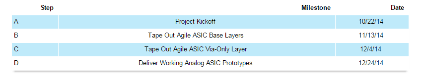
The customer reached out to Triad and we explained that with our patented Agile ASIC™ technology we could deliver custom analog ASICs on their requested schedule. The calendar for the project is shown below. The major milestones for the project are identified with the letters (A), (B), (C), and (D) on the the calendar.

(A) Agile ASIC Project Kick Off – 10/22/14
This Agile ASIC project started with a project kick-off meeting on October 22, 2014. At this meeting, the customer worked directly with Triad ASIC engineers to define the requirements for their ASIC. Following the kick-off meeting,
Triad’s IC designers got busy with two parallel paths.
One designer started working on the circuit level design using circuit IP from Triad’s extensive library.
The second designer simultaneously began the floor planning and layout of the complete chip using Triad’s patented Agile ASIC Tiles™. We will talk more about this process later but at high level Agile ASIC Tiles are IP that contain circuit elements and configurable routing fabric. These tiles can literally be ‘snapped together‘ during the floor planning process.
(B) Base Layers Tape Out – 11/13/14
In a radically new approach to chip design, Triad “taped out” or sent the IC design to the foundry well before the circuit was complete. Triad’s Agile ASICs utilize a patented via configurable methodology. Any of the analog or digital circuitry in an Agile ASIC can be reconfigured by changing a single via layer.
A custom IC consists of up to 30 mask layers with each layer taking 1-2 days of processing at the foundry. Normally, an ASIC cannot released until the entire design has been completed and fully simulated.
Triad’s agile approach allows the ASIC to be released early so that layers can be processed at the fab in parallel with the designers still working on circuitry and simulation.
(C) Via Layer Tape Out – 12/4/14
On December 4th, we taped out a mask for a single via-layer representing the circuit and routing between circuit elements. Since only this one via mask layer need be processed, the time left to get the chip through the foundry was only a couple of days. After fabrication was completed, wafers containing the ASIC die were shipped to a package house. At the package facility, the wafer was split into individual ASIC die. Each die was then placed into a QFN plastic package.
(D) Delivery of Working Agile ASIC Prototypes – 12/24/14
After the devices were packaged, they were overnight shipped to Triad’s facilities for testing and then devices were shipped to the customer for integration into their system for evaluation.
Custom Analog ASIC Project Milestones
What is an Agile ASIC™
Triad Semiconductor is North America’s premier supplier of mixed signal custom ASIC solutions. We design and manufacture custom analog and mixed signal ICs to customer specification. We are experts at full custom design and we have patented reconfigurable technology that is bringing true agility to the custom IC design process.
An Agile ASIC contains mixed signal resources that can be configured and interconnected by making a single mask layer change. An Agile ASIC contains analog and digital IP that is overlaid with a patented global routing fabric. Wafers containing Agile ASIC die are partially processed and staged at the semiconductor foundry. Only a single via mask layer need be changed to completely alter or reconfigure the functionality of the die.
Agile ASIC Benefits
- Major reduction in development time – Turn a one year effort into a 44 day quick turn project
- Fastest possible time to market
- Quick re-spin capability – 20 to 30 days
- Mitigated project risk – re-use proven IP and via reconfigurability
- Future proof – update design with a single via layer changed based on market feedback
This is a guest article by Reid Wender has been leading Triad Semiconductor’s marketing and application engineering groups since 2005. Prior to joining Triad, Reid was VP of Engineering for the Semiconductor Division at QuVIS, a leading digital cinema company. He has 20 years of ASIC design and project management experience at companies including Nextwave Silicon, ASIC International, Philips, and IBM. He holds a BSEE from the University of Tennessee.