

FlipChip Package Overview
If you were uncertain about the term “FlipChip” this tutorial will help you better understand what FlipChip packaging technology is all about.
FlipChip package technology has been around for 3-4 decades and started as a package solution for high pin count & high performance package requirements. At the beginning, the majority of FlipChip package applications were higher pin count SoCs (consisting of more than 700 pins), which a typical Wire-Bond BGA package type could not handle properly. In addition, some SoCs incorporated high speed interfaces (including RF) that wirebonds could not support due to the high wire inductance.
The demand for FlipChip package increased during the last decade and was driven by the mobile market, where package size and signal performance are critical.
Today, FlipChip package technology offer a range of benefits including: high pin count, high signal density, better power dissipation, low signal inductance, and good power/ground connectivity. FlipChip packages are quite popular today and you can find them in small devices such as cell phones where space is at a premium.
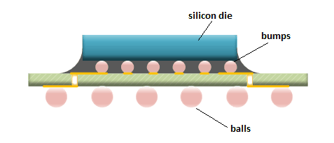
Figure 1: FlipChip Cross Section
Essentially, the name “FlipChip” describes the method used to connect a semiconductor die to a substrate. In a FlipChip package the dies are bumped and then “flipped” onto a substrate, hence the name “FlipChip”.
Thanks to the fact that the bumps are distributed across the entire the chip and not only located on the die edge, pads can be placed all over the surface of the die. This allows designers to place more pads per die, reduce the chip size, and optimize signal integrity.
The substrate provides the connectivity to the external PCB via solder balls. The substrate size, number of layers and material properties have direct impact on the total package cost. In some cases the substrate can be the most expensive element in a FlipChip package.
The bumps are placed directly on the I/Os pads and thereby connect the die to the substrate. Following the bumping process, the wafer is diced and finally, the bumped die is “flipped” on the substrate. The bumps connect the die and the substrate together into a single package.
Get even more details in our guide Flip Chip Technology Overview.
Substrate Technology
FlipChip substrate is a small PCB located inside the package and is very similar to any other PCB. The difference is that the substrate size is much smaller than most of the PCBs you have seen.
Substrate design consists of layout of all signals from the package external balls to the bump pads.
Substrates can be made by different materials: laminate, build-up, ceramic and more. Substrate layout design rules varies from different suppliers.
Substrates can consist of many layers ranging from 2-18 layers to allow routing of all signals.
Wafer Bumping Technology
Wafer bumps provide the connectivity between the die and the substrate by offering low inductance, low resistance and reliable and high quality production.
Wafer bumps can be composed from eutectic, lead tin, lead free, high lead materials, or Cu pillar. The bump size and bump pitch vary between the different assembly houses.
FlipChip Assembly Process
During the final processing step of the wafer bumping, the bumps are placed on the pads of the chip which can be found on the wafer’s top side. . In order for the chip to be connected or mounted to a substrate, the die is turned or flipped over and brought into alignment with the pads located on the substrate.
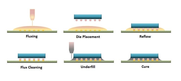
Figure 2: Steps in FlipChip Production
There are 6 steps in the process of creating a FlipChip which provides it with substantial versatility when connecting devices.
FlipChip Pros and Cons
There are advantages and disadvantages to FlipChip package, starting with the assembly method which creates a much smaller chip compared to previous wirebond solutions. Because the chip is directly connected to the circuitry board, the wires are shorter which creates less inductance. This means that devices can now pass signals at significantly higher speeds while dissipating heat more efficiently.
.

