

Guide to Semiconductor Wafer Sort
Wafer sort (or wafer test), is a part of the testing process performed on silicon wafers. Wafer sort is a simple electrical test, that is performed on a silicon die while it’s in a wafer form.
Wafer sort’s main purpose is to identify the non-functional dies and thereby avoiding assembly of those dies into packages. In many cases, wafer sort is a simple and quick test that focuses on a few electrical parameters that are most likely to fail.
Wafer testing is performed during IC production on every wafer and every silicon die. Otherwise, there could be defective semiconductor dies that will go through the assembly process and therefore lead to unnecessary expenses at the end of the manufacturing process.
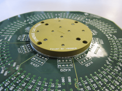
Photo: Probe Card (credit: Synergie-CAD)
One can imaging wafer sort as a financial decision that depends on yield, volume and packaging cost. But in some cases, companies perform wafer sort to monitor the silicon foundry yield. This feedback is then feedbacked to the fab to further optimize the silicon manufacturing process and hence improve the process yield.
A digital wafer map is attached to each wafer that has been tested to label the passing and non-passing dies.
How the Wafer Sort Works?
Called by different names such as the Electronic Die Sort (EDS), Circuit Probe (CP), and the Wafer Test (WT), This is the testing performed on the wafer or part of the semiconductor that carries the internal circuitry. Because the circuitry is so small, visual detection of any defects is virtually impossible. So, the testing itself is performed using specific equipment after the wafer has been created.
The wafer testing is done just before it is sent to the die packaging phase. The integrated circuits that are found on the wafer are checked for defects. The process uses test patterns to find any defects and thus eliminate the wafer from the next step in the process. The testing itself is performed by an ATE that has a wafer prober.
What is a Wafer Prober?
This is the device or machine that carries out the functions of the wafer sort or testing of the integrated circuits. How it works is rather simple. During the testing process the probe card which consists of several contacts that are microscopic in nature are located inside the wafer prober when the wafer itself is positioned for electrical contact. The wafer is mounted on what is known as a wafer chunk to keep it in position. The hold is vacuum-sealed which means that it is strong, but temporary so that another wafer can quickly be moved into position once the testing is over.
When each die has been tested electronically by the prober, it moves to the next die where another line can be tested. The prober will load and unload the wafer from the carrying device. Plus, it is equipped with optics for automatic pattern recognition so that the wafer is aligned properly for the testing process. That way the testing can be performed with the utmost accuracy and it ensures that a failure of any test is not due to the wafer being incorrectly aligned.
The contact pads on the wafer are touched by the tips of the needles from the wafer prober. This allows electricity to be properly conducted through the wafer which if successful completes the test so that the next line or circuit can be tested. However, if the electrical test does not pass through, the wafer is then moved from the manufacturing process for separate testing to ensure that it is defective.
The wafer prober can also handle multi-die packages like the System in Package (SiP) or the Stacked Chip-Scale Package (SCSP) thanks to the use of non-contact probes. This allows for the proper identification of the Known Tested Die (KTD) as well as the Known Good Die (KGD) which are vital to increasing the yield of the overall system.
Additional Testing
The ATE will also test circuitry along the scribe lines. Performance of the device can be rated when using line test structures. There are companies that get a good amount of information by using this process. There are some dies that include internal spare resources that are used for repairs such as found on flash memory IC. If some test patterns are not passed, the additional resources available can be used.
If there is no redundancy of the die that has failed in certain tests, then it will be discarded as useless. During the testing process, circuits that do not pass electricity are marked with a small ink dot located in the middle or the wafermap will store the information of failed or inactive circuits.
What is a Wafermap?
This is a map that reveals the dies that are passing and non-passing using bins. The bin itself will be defined as either good or bad die. The wafermap will then be sent electronically to the assembly house which only picks up passing dies by choosing the bin number that contains good dies.
In the past, the good dies were marked by ink dot, but this process is not common anymore. The use of ink dots allows for visual inspection as the operator can now disqualify a die based on the ink dot. While only dies that pass all the test patterns are used, there are cases in which one that did not pass all the test patterns can be incorporated if their flaws do not significantly interfere with the device where it will be placed.
After IC Packaging
The packaged chip will be tested another time during what is known as the IC phase. This testing process is very similar, if not actually the same as the original wafer test approach. While this might be seen by some as redundant, it does serve as an extra step that can catch a defects in the assembly process, for example, missing bumps or wirebonds.
This double-check helps keep defective dies from being sold or used in devices which creates considerable cost in detecting and replacing. However, there is considerable cost in the testing process, so it is not surprising that some companies that are producing a high yield of dies will skip testing altogether and risk blind assembly for greater efficiency.
Find here a list of IC testing companies.
Further reading: What is a ProbeCard?
Further reading: Understanding Semiconductor Testing
Further reading: IC Testing Overview
Further reading: Introduction to LoadBoard Design and Production

