Mobility Drives Thin Packaging
For the packaging industry, the smartphone changed everything, and experts agree that more changes— potentially big ones—are underway.
Bill Chen, a senior fellow at ASE Group, said when personal computers ruled chip demand, the main components had fairly standard package formats. The pace of change has picked up in the smartphone era. Now, “the people who design smartphones compete by the functions they can provide, and probably more importantly, by how they look. You want them to be thin, and you want all the functions.”
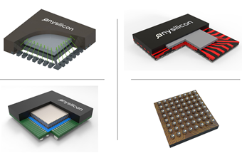
That need for thin packages drove the industry to wafer-level chip-scale packages (WL-CSP), a hybrid between front-end and back-end processes in which solder balls are created beneath the chips before the wafer is diced. ASE estimates that about 30% of the die in smartphones now are in WL-CSP packaging, nearly all in a fan-in configuration in which the solder balls are spaced out directly underneath the die.

According to industry research firms Yole Developpement and System Plus Consulting,approximately 30% of the chips in 3 of the market-leading smartphones use wafer-level chip-scale packages.
Jan Vardaman, president of the packaging consultancy at TechSearch International (Austin, Texas), said Apple’s first iPhone used 2 wafer-level packages (WLPs) in 2007, but today’s much-thinner iPhone 6 has about 26 WLPs. “Several years ago, Samsung did not use WLPs in its mobile phones,” Vardaman said. “Today, around a dozen WLPs are found in the latest Samsung smartphone. Even the latest portable communication gadget, the Apple Watch, contains as many as a dozen WLPs.”
Traditionally, WLPs have been used for devices with low pin counts and small die sizes. The number of chips packaged in fan-in WLPs is still growing: TechSearch predicts a nearly 9% CAGR for the 5-year period from 2014 to 2019.

Fan-in wafer-level packaging is prevalent in relatively low pin count ICs used in mobile phones. Fan-out wafer-level packaging is gaining momentum for higher pin count devices. (Source: Yole Developpement.)
Underway is another significant evolution that could shake up the chip industry. Fan-out wafer-scale packaging, some experts believe, could push down the share held by flip chip packages and push out the need for the more expensive 3D through-silicon vias (TSVs) in consumer applications, including smartphones. Outsourced semiconductor assembly and test companies (OSATs) and foundries alike are scrambling to provide this next significant wave of packaging innovation. (See sidebar: Fan-Out Is a Game Changer.)
Fan-out packaging already includes a high-density (HD-FO) category, with sub-10nm lines and spaces. The advanced fan-out processes, and TSV connections, are pushing Applied Materials and other tool makers to develop new techniques that can be used for 300mm, 200mm, and smaller wafer sizes.
“We want to push our tools and see how far they will go,” said Mike Rosa, director of strategy and technical marketing for emerging technologies at Applied. “One challenge with the increasing device density on thinner wafers is dicing. The dicing lanes are becoming smaller, and if there is any chipping it can impact the active area on these small die,” said Rosa.
Rosa added that Applied is “pushing the limits of conventional TSV processes to accommodate the trend toward smaller CDs and higher aspect ratio TSVs.”
OSATs ADOPT PROCESS CONTROL
The rise of wafer-scale packaging, where front-end-like steps are used, has been a big part of the transformation of the OSAT sector. “More packaging-style processes are being completed in the ‘front end.’ The line between front- and back end is being blurred with the growth in technologies like wafer bonding,” Rosa said.
Shekar Krishnaswamy, a senior manager of Advanced Productivity Solutions at Applied Global Services who works with OSATs on factory automation issues, said the OSAT factory is becoming more fablike, with more packaging-style processes being completed in the traditional front-end. “The OSATs are using wafer fab equipment and technology—lithography, etching, plating, CMP, and others. Certainly the automation solutions [they use] are essentially the same [as front-end fabs].”
Gone are the days when packaging plant workers would tend to long rows of humming, clacking wire bond machines. And OSATs are putting in the same manufacturing execution, material handling, and process control systems long used by front-end wafer fabs in order to maximize return on their assets.
“The OSATs have had to quickly change,” said Krishnaswamy. “End customers now are asking their OSAT suppliers to provide the same kinds of advanced process control (APC) and yield tracking tools as the wafer fabs. As customers turn to more complex processes, such as fan-out wafer scale packaging and TSVs, those process control demands are set to increase,” he added.
Indeed, while integrated device manufacturers (IDMs) once did almost all their own wafer probe testing, for example, now that important function often is done by the OSATs. To leverage their investments in expensive test computers, OSATs use one test head for wafer probing and another for final test after assembly is completed. “The same expensive test computer can be used one day as a prober, and another day with a different handler for final test. The OSATs have become very good at extracting value from their physical assets,” Krishnaswamy said.
| Speaking at the 2015 Advanced Process Control (APC) conference, Thomas Sonderman, vice president of the software business unit at Rudolph Technologies, Inc. (Tewksbury, Massachusetts), said OSATs are scrambling to modernize their automation processes. |
In an overview of the last 25 years of APC, he noted that the big system companies are seeking to link their entire supply chain together, using dashboard-style displays to manage the flow of components.
“A lot of information gets generated, including wafer-fab and assembly-and-test information. The goal is to link all of this together. We need data democracy, and we need to think about how to prevent barriers in the first place,” said Sonderman, who previously worked in APC development at GLOBALFOUNDRIES.
“In China, the OSATs have the mindset that ‘if our customers want APC and fault detection, we want it.’ They have the motivation, but they don’t necessarily want to give you a lot of money for it.” Sonderman added that the Chinese OSATs prefer off -the-shelf process control and automation solutions. “They don’t want to build an army [of internal software developers],” he said.

Early in his career, ASE’s Chen helped develop IBM’s pioneering C4 chip packaging technology (C4, or controlled collapse chip connection, was an early flip chip technology that involved depositing solder bumps on the top side of the wafer during final wafer processing). He said the back-end processes are picking up the pace as Moore’s Law scaling becomes more difficult. “Speaking from the packaging side, I would say the back end is no longer at the back end. We are at the front of the whole effort of getting semiconductors into systems. Now, what we do is much more application specific and customer specific.”
Rozalia Beica, chief technology officer at Yole Developpement (Lyon, France), concurred, saying the advances in packaging technology have provided the semiconductor and systems companies with more flexible ways to advance their products. “With Moore’s Law slowing down at the advanced nodes, things are getting more expensive and yields are becoming more difficult to achieve. So many companies are using, say, 65nm technology and not 14nm technology. They are using advanced packaging to put the right solutions together without trying to do everything on 300mm wafers at the most advanced nodes.”
SMALL FORM FACTOR SOLUTIONS
One of those companies is Silicon Labs (Austin, Texas), which combines microcontrollers, low-power radio frequency (RF) circuitry, and on-chip flash memory into products aimed at Internet of Things applications. (See “Silicon Labs Tackles IoT Solutions,” Nanochip Fab Solutions, Vol. 10, Issue 1, 2015.)
| . |
Daniel Cooley, Silicon Labs’ vice president of marketing for IoT products, said many of the chips used in IoT or wearable applications are extremely small. For example, a recent 8-bit IoT controller from Silicon Labs is in a chip-scale package (CSP) with a 1.8 by 1.66mm footprint, which is about one-fourth the footprint of a conventional quad-flat no leads (QFN) package.
“With the IoT, you have to keep costs down. But you also have to get all of the IOs out in a small form factor product, and that is a hard process. There is a lot of current going through very small pipes: 300 or 400 milliamps while transmitting. Doing that in a small form factor is hard,” Cooley said.
Over the past two years, the major OSATs have improved their ability to handle the very small CSPs, with small solder ball pitches. “Two years ago, handling .5mm pitch balls was expensive, but now it is standard. In fact, no matter what factory you are in they can handle .4mm pitches now. From the viewpoint of fan-in CSPs, standardization on the .4mm pitch has been nice,” Cooley said.
Improvements are still needed. “The OSATs could make CSPs more tolerant of the probe process. That would be a big step forward. The probe card has to push down the pogo pins, and CSPs are very sensitive to any deformation on the landings. It would help if the CSPs could be more tolerant of any deformation during probe test,” Cooley said.
WATCHES AND WEARABLES
The entire wearables category is prompting closer collaboration, with packaging decisions made early in the design cycle with packaging partners. Cooley said Silicon Labs is learning that chips used in wearables are “a little more complicated” in terms of flexibility and thermal constraints. Also, “wearables all connect to your phone, so there is a need to optimize for the antenna radiation pattern. And the package has to be able to adapt to a wide array of PCB materials.”
Dick James, a senior fellow at reverse-engineering firm Chipworks (Ottawa, Canada), said his company did a teardown of the Apple Watch recently. While most of the chips are in fairly standard packages of one kind or another, the entire PCB board is encased in an over-molded cover to prevent moisture and radio frequency waves from compromising the watch.
“That is the first time we have seen that total encapsulation, and we think they did that because it is a wearable and likely to see moisture ingress challenges. RF shielding is also needed. In the unlikely event of sticking it in a microwave, the shielding could prevent the watch from exploding,” James said.
THINNER MEMS SENSORS
Rosa, who earned his doctorate in the MEMS field, said the move to thinner MEMS sensors in smartphones is having a major impact.
“MEMS are a special challenge, because the package often includes the MEMS device, a layer of control logic, and a capping layer. The whole structure might be 300 microns, so all those layers need to be thinned.”
In part, that need motivated Applied Materials to offer customers a series of modifications to its Endura platform, enabling the handling of wafers down to 100 microns thick. “It should be noted that in most cases, customers are not passing around super-thin wafers. The customers usually bond the wafer to be thinned to another wafer, either glass or silicon, before thinning,” Rosa added.
Applied is participating in research and development efforts in Singapore and Europe to reduce the size of the TSVs. TSVs are used to connect the MEMS and ASIC wafers in back-side-illumination (BSI) CMOS image sensors, some power ICs, and in several other applications. To reduce stress, polysilicon vias are often used, and the number of TSVs in these applications is small, sometimes only 6 to 10, to connect the MEMS structure with the control logic wafer, or to connect the MEMS to the PCB, Rosa said.
One motivation for TSV use in these devices is to get away from wire bonding, where the pads take up valuable real estate. “If a customer goes from wire bonds to TSVs, they can save 25 to 30% of the die area. That is huge. They can increase the numbers of die per wafer by 25 to 30% with TSVs,” he said.
With an overall goal of putting more TSVs into a certain area, researchers are investigating how to make the critical dimensions of the TSVs smaller, with a smaller diameter and a higher aspect ratio (width to depth).

A TSV-last process flow for MEMS devices is suited for outsourcing to an OSAT, and has relatively low stress between the via and silicon. (Source: ASE Group.)
“As chips get smaller, the CD of the TSVs decreases, and that increases the challenge of how to perform a reliable line-and-fill without voids. If the diameter goes from 10 to 5 microns, we really have to improve the barrier and seed layers,” Rosa said.
The thickness of the barrier and seed layers correlates strongly with the quality of gap fill, which is related to the choice of chemistry, hardware, and process control capabilities.
For a detailed discussion of TSV processes, see “Optimizing TSV processes and integration for volume manufacturing” by David Erickson, Isaac Ow, and Sesh Ramaswami (all of Applied Materials), Chip Scale Review, January–February 2015.[1]
TSVs FACE COMPETITION,NEED TIME
Gaurav Sharma, a senior member of the technical staff at GLOBALFOUNDRIES, joined that company this year after spending more than a decade in various advanced packaging operations.
Sharma said TSVs—both in interposers and in vertical 3D ICs— are gaining more traction from a production point of view. “TSVs are in volume production, but for niche applications,” he said, noting that high-bandwidth memory graphics, and very high performance ASICs are turning to TSVs.
An area where TSVs provide advantages is for the “huge bandwidth requirements coming up with Internet traffic,” Sharma said. While these applications do not have volumes nearly as high as devices used in mobile systems, he believes “there is serious interest in 3D TSVs by some pretty significant players who want to bring this technology into production.”
The challenge facing TSV adoption arises from the relatively high cost of the complex process, especially compared to the up-and-coming HD-FO chip scale packages. “When we look at TSVs for mobility, there are alternative technologies that can do much the same thing at a much better price. It is a problem of there not being a business need. Why would you pay significantly more when the product requirement can be satisfied by advanced packaging that is more cost-effective?” he asked.
Sharma noted that designers also are hesitant about 3D TSVs, which require that the active silicon circuits be designed around a keep-out zone occupied by the TSVs. “What I have learned from various customer engagements is that designers are resistant to this idea,” he said.
Rozalia Beica, the Yole CTO, believes 3D TSVs will gain a stronger foothold, but it will take time. “I personally am a strong believer in TSVs and have worked on them since 2006,” she said. “If you look at other technologies, flip chip was developed by IBM in 1960, but it didn’t go into volume production until 1980. Similarly, the time for MEMS to go from development to mass adoption took 20 years. TSV technology is not slower; it is just that there was such big hype around it that now everyone is waiting for it to be adopted.”
Indeed, companies ranging from AMD to Xilinx in logic, and SKHynix and Toshiba in memories, have introduced products that include some form of TSVs. “Personally, I don’t think TSVs are necessarily slower [to proliferate] than other technologies,” Beica said.
[1] “Optimizing TSV processes and integration for volume manufacturing”: http://www. chipscalereview.com/issue/1501/ ChipScale_Jan-Feb_2015_v8-digital. pdf#page=34
_______________________________________________________________________________________
This is a guest post by Mike Rosa PhD, director of strategy and technical marketing for 200mm products at Applied Materials.