Moortec Opens New European Design Centre in Poland
The brand new facility will be headed up by Moortec Design Centre Manager, Szymon Gerka, with support from Moortec CTO, Oliver King.
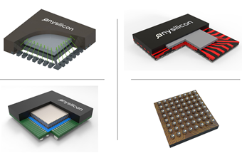
Moortec provides compelling embedded IP subsystem solutions for Process, Voltage & Temperature (PVT) monitoring, targeting advanced node CMOS technologies from 40nm down to 7nm.
“The exciting new Design Centre in Gdańsk will allow Moortec to accelerate its engineering efforts in terms of its advanced node roadmap and help cement its position both in Europe and Globally as the number one provider of embedded PVT sensing technology”. – Oliver King, CTO Moortec Semiconductor. “We also recognise the valuable, highly professional and talented engineering resource that Poland has to offer.”
The recent rapid growth of Moortec means the company is seeking talented engineering staff to grow its team in Poland. Moortec wishes to recruit designers to help ensure the company continues to provide cutting edge embedded monitoring IP for the advanced node semiconductor industry.
“We are looking forward to growing the team and continuing to provide highly accurate, highly featured monitoring IP to optimise the performance and reliability of today’s modern SoCs whether that be for consumer, telecommunications, datacentre and enterprise applications or for emerging markets such as automotive, IoT and AI”. – Ramsay Allen, VP of Marketing Moortec Semiconductor.
Moortec’s PVT monitoring subsystem IP is designed to optimise performance in today’s cutting-edge technologies, solving the problems that come about through scaling of devices. The new design centre will strengthen Moortec’s engineering team and allow the company to add even more new silicon-proven designs to their already impressive IP portfolio.
About Moortec Semiconductor
Established in 2005 Moortec provides compelling embedded sub-system IP solutions for Process, Voltage & Temperature (PVT) monitoring, targeting advanced node CMOS technologies from 40nm down to 7nm. Moortec’s in-chip sensing solutions support the semiconductor design community’s demands for increased device reliability and enhanced performance optimization, enabling schemes such as DVFS, AVS and power management control systems. Moortec also provides excellent support for IP application, integration and device test during production.
For more information please contact Ramsay Allen [email protected], +44 1752 875133, visit www.moortec.com and follow us on Twitter @moortec and LinkedIn.