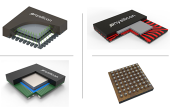
BGA substrate Design
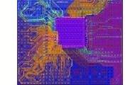
Quite often with the development of a new ASIC, a new BGA substrate is required. The process of designing a BGA substrate is actually very similar to PCB design. The only difference between the two design features is that a BGA substrate is typically much smaller than any other PCB design and as a result it’s important to utilize some type of EDA tools for the design process. This ensures that any type of BGA substrate design will be properly produced.
BGA substrate design also follows design rules provided by the assembly house, the design of a BGA substrate can be done by the assembly house or by a 3-party contractor.
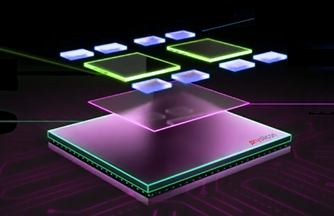
A BGA substrate is essentially a carrier that’s use with many types of BGA package. For complex devices like microprocessors a BGA substrate needs to provide many different interconnection pins and a process for designing all of these pins and integrating them into the package can actually be extremely complicated. Some of the BGA substrate design consideration includes: Utilizing shorter leads, power planes, signal integrality, RF performance etc.
Quite a large number of BGA substrate designs are handled by automated processes. Because so many pins are required and because it’s much easier for a computer to determine the shortest path for every pin, quite often this is done through an EDA design software. While there is definitely a human interface when it comes to editing the high-density designs, today quite a lot of BGA substrate design is handled primarily by computers and software.
BGA designs need to not only create the fastest possible integrated circuit with hundreds of different pins and arrays, but the design also needs taken to consideration heat conduction, unwanted inductance, the difficulty of inspection on every developed part and the cost for production.
A lot goes into the design of any BGA substrate but with proper design one can ensure a better functioning ASICs and more reliable products.
Read more about BGA Substrate Design here.
Click here to find IC Package Design Companies.