FD-SOI
As we move further into the modern times, we can begin to notice certain trends in the development and advancement of technology. We are surely and rapidly moving towards a world where technological devices and gadgets not only continue to exponentially improve in terms of their performance, but also become significantly reduced in their size and power consumption. Technology keeps becoming better, more powerful, and much smaller. The goal here is to extract the maximum degree of performance out of minimum possible energy and space consumption so as to make processes efficient. FD-SOI technology works on a similar principle.
What FD-SOI?
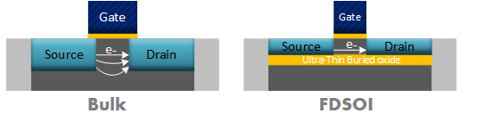
FD-SOI stands for Fully Depleted Silicon On Insulator and it is a planar process technology that, when compared to traditionally used bulk technology, offers a much greater and more efficient transistor function and properties. It can, essentially, be considered to be a simplification of Silicon on Insulator, or SOI. An FD-SOI is made from two very thin layers that collectively form the ultra thin body and buried oxide Fully Depleted SOI, or UTBB-FD-SOI. The first layer is that of buried oxide, an insulator that lies on top of a thin base silicon, which is the second layer and implements the transistor channel. The reason why this transistor is termed as ‘fully depleted’ is that it is so thin on a whole that the channel does not need to be doped.
FD-SOI Benefits
One of the major benefits of this kind of a transistor is that it prevents the leakage of performance draining currents as the buried oxide insulating layer traps the electrons growing from the source to the drain, as well as lowers the capacitance between the two stages. In conventional bulk technology, the absence of the ultra thin oxide layer means that the current can be lost and dissipated as it travels from the source to the drain, resulting in unnecessary loss of power and energy, and an inefficient system.
Another reason why FD-SOI may be preferred over traditional tech setups is that it offers body biasing, a feature that is very limited and rarely found in bulk technology due to its current leaking properties. The insulating layer not only enables the biasing feature, but also allows the user to apply higher biasing voltages so as to gain a better dynamic control over the transistor. The biasing enables the user to partake in quick switching and also ensures that compared to its performance, the energy consumption is much lesser than traditional systems, making it much more efficient.
The transistor can be decreased in size down to a 10nm large body, making it an extremely low space occupying yet incredibly powerful and efficient system. It is also much less riskier to develop which is why it gives better value for the cost invested in it.
FD-SOI technology is finding its use in the automotive industry in particular, considering its ability to tolerate radiation. Not only that, but this innovative and useful piece of tech is also expected to make waves in the modern market due to its relevance and association with the Internet of Things and its various components.