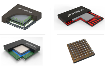
Semiconductor Packaging
Semiconductor packaging can vary based off of the component requirements of any device. Semiconductor packaging is designed to provide ongoing protection against corrosion and impacts. The packaging also works to hold any of the contact pins and leads for connection of external circuits to the main device as well as manage heat through the device. There are thousands of different industry-wide standards and packaging types available in the most popular materials include ceramic casings, glass, plastic or metal.
Semiconductor packaging may carry hundreds of connections in an extremely complex manufacturing system. Packaging that is extremely durable actually works to protect devices from stray particles, moisture and other environmental factors that can cause inefficiencies and even failure. As a result manufacturers need to consider the applications that they are designing technology for and create packages that can stand up to even the most extreme situations.
When it comes to manufacturing semiconductor packaging and actually identifying it, manufacturers of packaging generally use ink logos or laser marking to etch a part number and any number of codes on every packaging material. This ensures that future manufacturers can discern the exact material as well as distinguished the types of compatible and incompatible devices with pre-manufactured packages. A two digit week number is also generally included so that technology developers can see exactly when the packaging material was created.
Semiconductor packaging standards are heavily monitored through international industry associations. Pro electron, JEDEC and EIAJ ensure that manufacturers continue to produce the same high quality products that will ensure the future success of technology developers.
There are still a huge number of innovations being made in this market. Semiconductor packaging now can include many special features such as light emitting or light sensing capabilities, ultraviolet erasable programmable read-only memory is possible through quartz semiconductor packaging.
It’s these types of innovations that could lead to the technology that will bring us into the future of mobile devices, computing and more.