TSV Integration is Creating Growth
“The long term growth of the equipment & materials business will be supported by the expansion of 3D TSV stack platforms” says Yole (Yole Développement) in its latest report, “Equipment & Materials for 3DIC & WLP Applications“. The market research and strategy consulting company, Yole proposes a deep analysis of the equipment & materials market for 3DIC & WLP applications. Under this new report, analysts announce a market multiplied by 2.5 in the next 5 years…
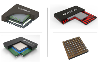
Equipment & Materials for 3DIC & WLP Applications report presents an overview of the main equipment and materials used in the 3D & WLP applications. Under this technology & market analysis, Yole’s analysts describe insights on a number of equipment tools, breakdown by wafer size & revenue, by type of equipment & materials and advanced packaging applications. Moreover, they also provide a detailed analysis dedicated to key suppliers, market shares and technological highlights that impact the 3D & WLP industry. Equipment & materials market forecasts are calculated from 2013 to 2019.
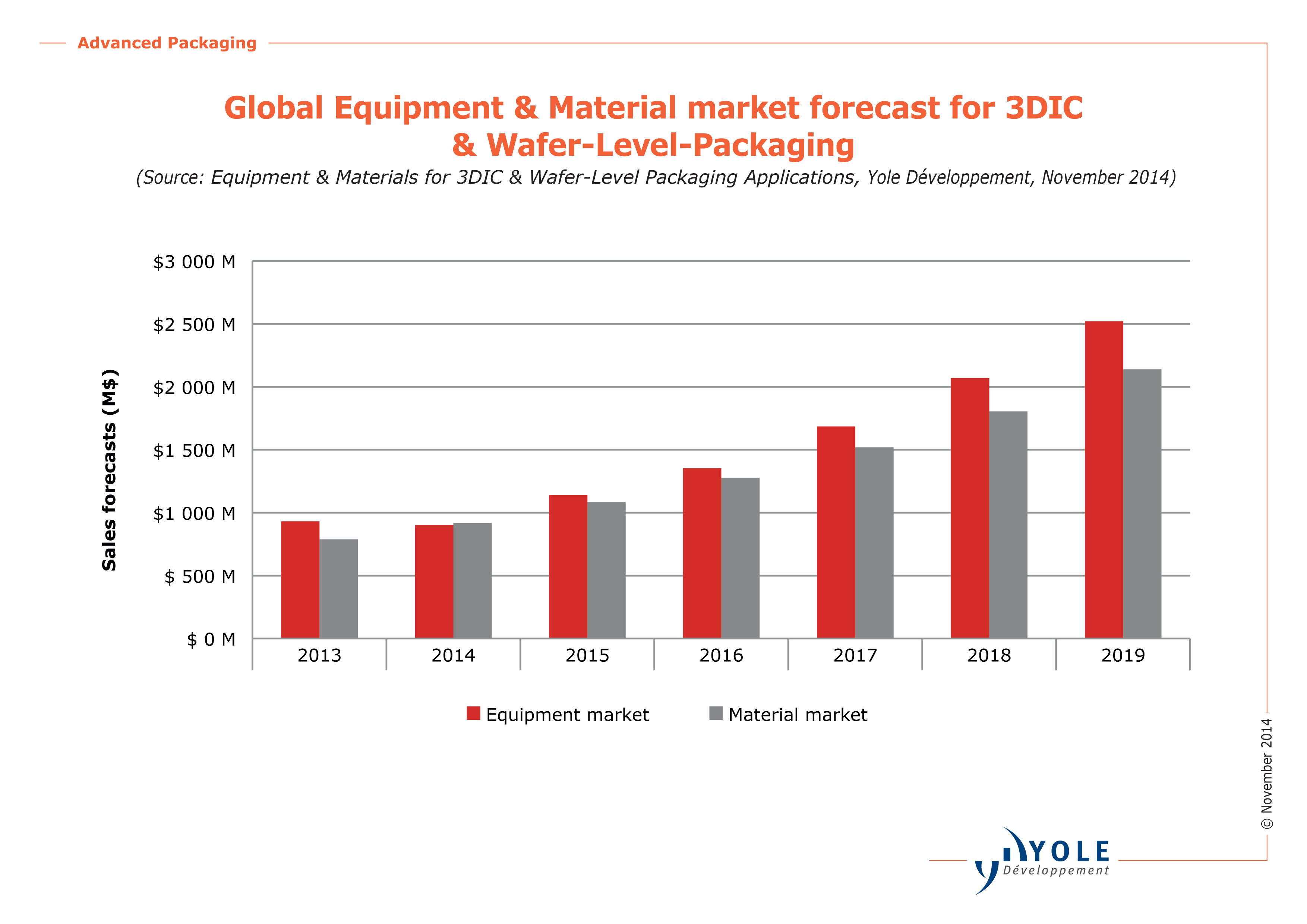
“Mainly supported today by flip-chip wafer bumping, the equipment market generated revenue of more than $930M in 2013” announces Amandine Pizzagalli, Technology & Market Analyst, Advanced Packaging & Semiconductor Manufacturing, Yole. “It is expected that this equipment market revenue will peak at almost $2.5B”, she adds. This market is fueled by the 3D IC technology with TSV interconnects, an area offering opportunities for new developments in equipment modification— equipment that is much more expensive than the tools used for established Advanced Packaging platforms :3D WLP, WLCSP and flip-chip wafer bumping. Indeed, according to Yole, 2015 will be the key turning point for the adoption of 3D TSV Stacks since the memory manufacturers, such as Samsung, SK Hynix, Micron, have already started to ship prototypes this year and might be ready to enter in high-volume manufacturing next year.
In its latest announcement (Source: Song Jung-a, Financial Times), Samsung Electronics reveals its $14.7 billion investment, to build a new semiconductor plant in South Korea. This investment becomes the biggest single expenditure on a memory chip factory.
According to the Korean company, construction of the world’s biggest plant will begin in the first half of next year and complete in the second half of 2017. In addition, logic manufacturers will diversify investments from System-on-Chip to Package-on-Package and will benefit from Advanced Packaging platforms such as 2.5D interposer and FOWLP to stimulate their high-volume production.
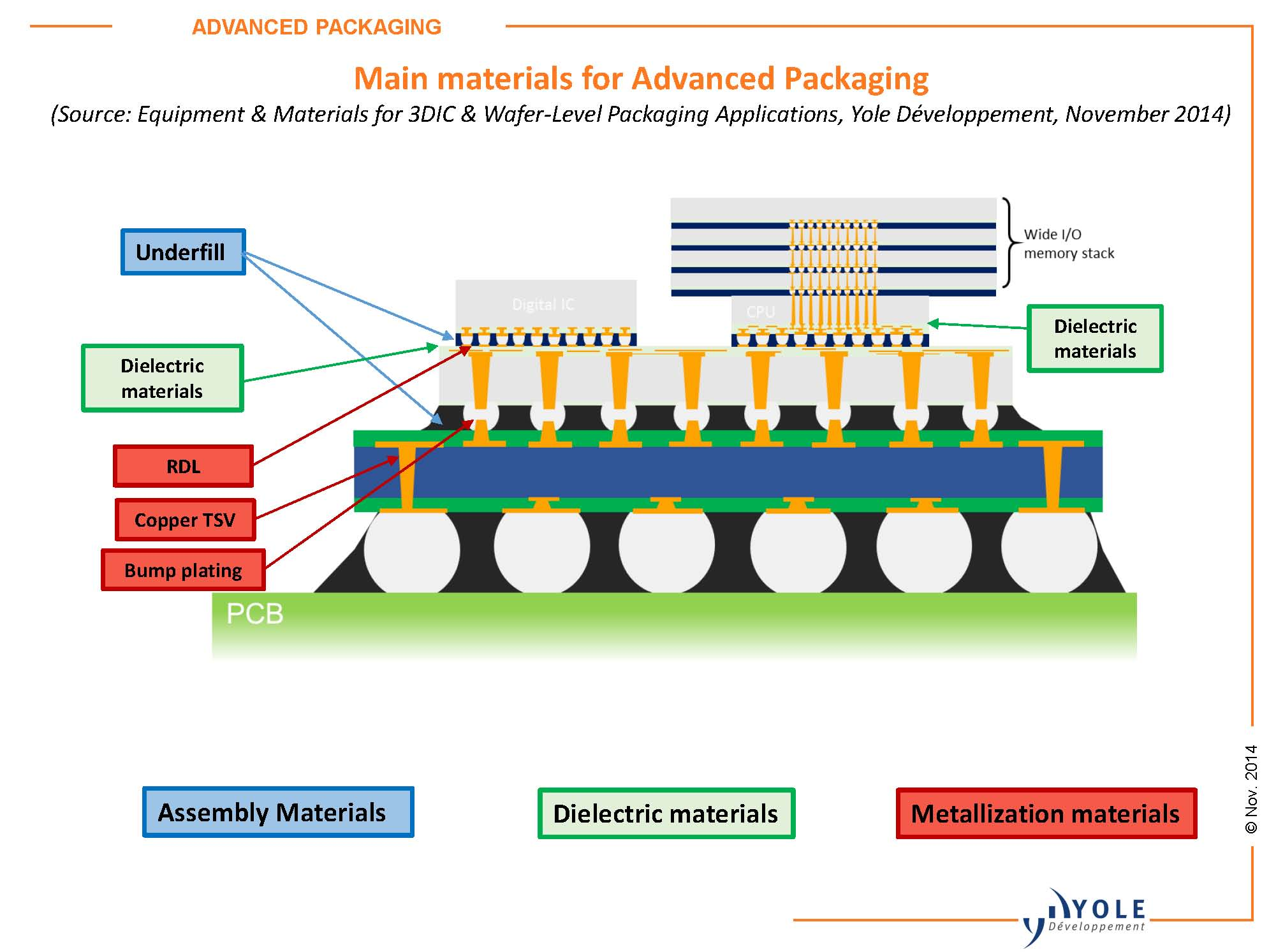
From the materials side, Yole confirms: “The materials market will grow from $789M in 2013 to over $2.1B with a CAGR of 18%”. Growth will mainly be driven by the expansion of the next generation Wafer-Level-Packaging platforms: 3D TSV stacked memories, multi-layer RDL for FOWLP & WLCSP. Such platforms are becoming more complex and requiring additional and various thin layers, as well as advanced materials, to achieve better performance.
More information about Advanced Packaging reports is available on http://www.i-micronews.com/advanced-packaging-reports.html
______________________________________________________________________________
This is a guest post by Yole Développement that provides marketing, technology and strategy consulting.