

The Ultimate Guide to QFN Package
QFN Package Overview
The QFN (Quad Flat No-lead) package is probably the most popular semiconductor package today because of four reasons: low cost, small form factor and good electrical and thermal performance. In this article we will provide an overview to QFN packaging, discuss QFN package technical details and specifications in detail and present various versions of QFN package that are used in IC packaging.
Like any other semiconductor package, a QFN package functionality is to connect (both physically and electrically) silicon dies (the ASIC) to a printed circuit board (PCB) using surface-mount technology. QFN is a lead frame-based package which is also called CSP (Chip Scale Package) with the ability to view and contact leads after assembly.
QFN packages typically use a copper lead frame for the die assembly and PCB interconnection.
The QFN package can have a single or a multiple row of pins. The single row structure is formed either by a punch singulation or a saw singulation process, both of these methods divide a large array of packages (for example a 18” x 24” sheet) into individual packages. The multi-row QFN uses an etching process to realize the wanted number of rows and pins; these are then also separated, typically by saw.
QFNs have an exposed thermal pad at the bottom of the package that can be soldered directly to the system PCB for optimal thermal transfer of heat from the die.
QFN benefits include a decreasing lead inductance due to optimally short bond wires, light weight, thin profile and small sized “near chip scale” footprint. The QFN package is perfect for many new applications that need better performance in size, weight, thermal and electrical properties. The potential downsides of adopting QFN packages include a possible floatation on the pool of molten solder under the thermal pad during assembly; oxidation problems of the exposed chip contact pads; missing clearance of a soldering pencil to reflow pads under the chip if touch up is desired. These issues can be mitigated by better control of the re-flow process and using QFNs which are plated (tin common) to lessen oxidization issues.
Wire Bond QFN vs. Flip Chip QFN
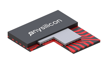
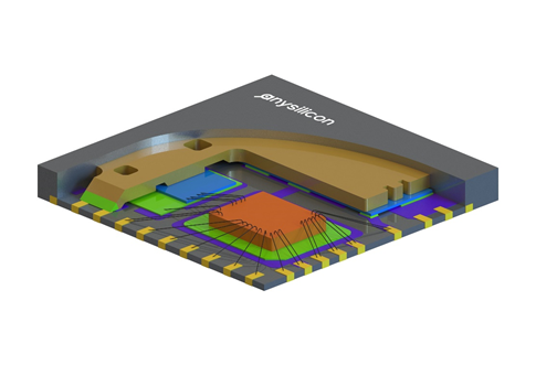
Although a wire bonding is the most common method for die to package connectivity, some packaging houses offer a flip chip QFN version as well. A flip chip QFN provides better electrical performance and typically used in RF and wireless applications. The following figure shows a typical Flip Chip QFN package, where the die is already bumped and thereafter “flipped” on the leadframe. The red traces in the drawing represent the leadframe.
Flip Chip QFN requires a bumping process in addition to the typical assembly steps, therefore in most cases Flip Chip QFN cost will be on the high side.
Punched vs Sawn QFN
Higher volume production tends to support sawn type QFN, whereas punch type is often seen with lower volume products. Both have very similar electrical and thermal properties. The drawing below show the package structure difference between a punched and sawn QFN.
The naming are based on the singulation method, where punched QFN is separated by a punch tool and a sawn QFN is separated by a sawing a large amount of packaging into single units.

QFN LeadFrame Overview
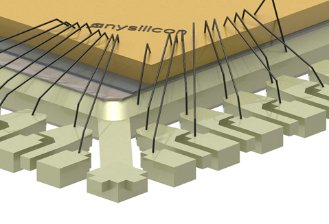
Every QFN package consists of a LeadFrame, which is a copper frame surrounding the die and consists of all the package pads (fingers) and the exposed pad. A leadframe is typically made as a large flat sheet of copper with 0.3-0.4 mm thickness with Matt Tin coating. The sheet goes through a Photochemical etching process to remove the unnecessary area. Next, the edged sheets are diced into strips. The inner leads are used for wire bonding and the outer leads are used as the QFN package leads.
In the assembly process the leadframe strips are going through a stamping process. When the stamping process is completed, the assembly process can start. A wire bonder will then connect the die pad to the leadframe pad and of course add optional downbonds from the die to the exposed pad for grounding.
Unused leadFrame shelf life time at packaging assembly house is approximately 1 year; this means that after one year, the packaging house will ask you to pay for making new LeadFrames for your QFN package.
Read about “Lead Frame Overview and Custom Lead Frame Benefits“.
QFN Thermal Characteristics
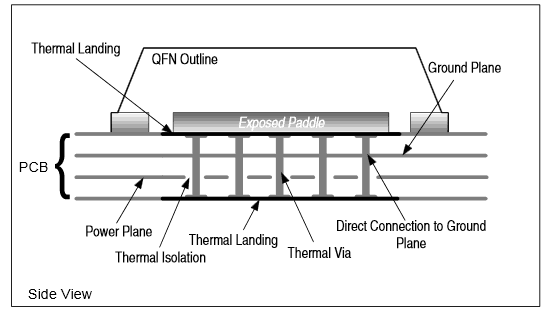
The QFN package exposed pad (or paddle) offers a low thermal resistance path for heat transfer to the PCB and therefore it’s recommended to solder the exposed pad to a large conductive surface such as GND plane. This path carries approximately 70% of the heat away from the Package. With the presence of metal plane the heat flow via the exposed pad can increase to 90%.
Source: http://pdfserv.maximintegrated.com/en/an/AN862.pdf
QFN packages allows for good electrical and physical connection in between the PCB and the IC, thanks to the metal vias in the thermal pads that facilitate the heat transfer. There are different types of QFN. Two of the most common are: air-cavity QFNs (made of three parts such as: copper leadframe, ceramic or plastic-molded body, and either a ceramic or plastic lid) and the plastic molded QFN (characterised by being fully molded with no air in the package).
QFN Electrical Characteristics
Thermal pad, or exposed pad, is an efficient method of drawing heat from the die to the PCB. QFN is a thermal efficient package and the exposed pad is a very cost-effective solution. QFNs can handle up to 2W-3W without forced air cooling.
Different manufacturers call these packages with different names such as MLF (micro lead frames), FL (flat no lead), they are available with pads on only two sides as well as the more typical four sides.
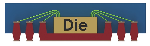
QFN Bonding Diagram
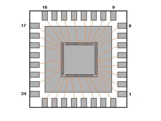
When the QFN package design needs to start the assembly house will ask you for a few documents. One of them is the bonding diagram that shows the connectivity between the die and the package pads. The bond diagram shows an example for a 16 pin QFN. The short wire bonds are indication to down bonds e.g. interconnect to the exposed pad.
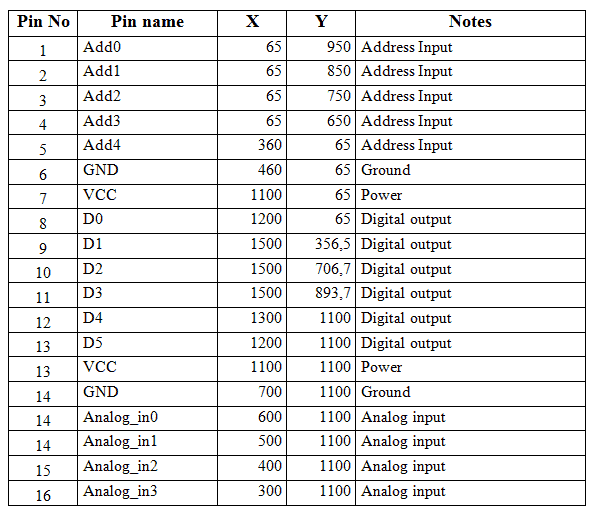
an additional document that is required, is a netlist that describes the die to pad connectivity that consist the die coordinates. The following table shows a netlist for 16 pin QFN.
QFN Marking Specification
QFN package is relatively small and therefore does now allow much space for legible marking. A 5mm x 5mm QFN can have up to 5 or 6 characters in one line; 3 or 4 lines are possible.
Wire Bonding
Gold wirebonds were the default material for many years. They are still available but are being replaced by copper. Copper wirebonds have lower cost and offer better conductivity. Yet copper wires require more force to bond the wire to the pad. Many semiconductor foundries supply IO pad cells designed to support copper bonding as a thicker pad is usually needed.
Die Attach
This is the epoxy material that fixes the die to the leadframe pad. Two main types are used, conductive and non-conductive, depending on the systems electrical requirements; electrically conductive materials (i.e. silver-loaded epoxy) tend also to have better thermal conductive properties.
Other Names for QFN
While most of the assembly houses provide QFN packaging services, they use different names.
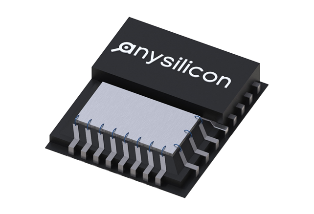
Multi-Row QFN Package
In applications that require high pin count, Multi-Row QFN could be the perfect solution. Multi-Row QFN (or aQFN) offers multiple rows of pins, very similar to BGA technology, and in most cases offer also lower cost. This package type is still based on wirebonds, uses a lead frame, and offers up to 400 IO pins. Soldering a multi-row QFN to a PCB will require a reflow process (like BGA package).
In the following figure a bottom view of a dual raw QFN (aQFN) package is shown. From the bottom, this type of package is similar to a BGA package, and indeed it offers a large number of I/Os compared to a conventional QFN package. Typically a dual raw QFN package will cost less than a BGA because it’s based on a leadframe rather than a substrate.
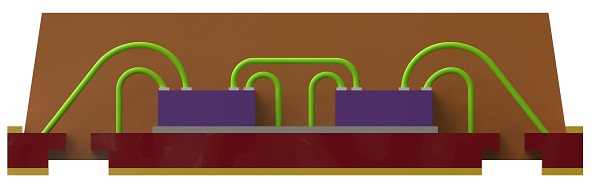
PQFN Package
The PQFN (Power Quad Flat No-lead) is a QFN package type that is suitable for power applications. Power Quad Flat No-Lead (PQFN) is an SMT semiconductor technology designed for PCB-mounted applications. JEDEC, has given a registered designator of MO-251 to describe the this package type.
Depending on the requirements and intended application, PQFN packages consist of either a single exposed pad or multiple exposed die pads. In addition, PQFN package offers full package customization to address both power and electrical requirements – e.g., the number and size of exposed pads are fully customized as well as the size and location of the heat slug.
PQFN package offer multiple exposed pads structure as shown in the below figure. This feature is beneficial in cases when silicon elements are using different grounding, or need connect another potential (voltage) to the exposed pad for heat dissipation. The exposed pads are fully customized in terms of size and shape together with the lead frame.
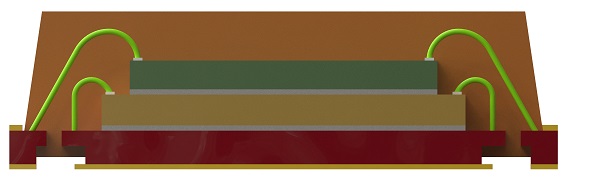
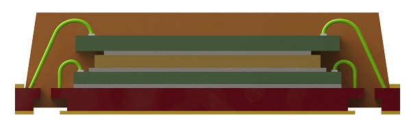
Multi-Die QFN (System in Package)
Although QFN package consider small size, it can, in many cases fit 2 or even more dies into a single package. The following 3 drawings show various multi-die package strategies: stacked and side by side.
Need a price quote for your QFN packaging? Get 3 quotes quickly using this form.

