Understanding Antenna in Package Design
Antenna in Package (or AiP) is an new trend in IC packaging which is an enabler of smaller and high integrated ICs that consists of ICs and Antenna inside a package. Antenna in Package allows integration of all the complex RF components, together with the base-band circuitry into a complete self contained module greatly facilitates the work of the system integrator. The system integrator no longer needs to design complex RF circuits at the application PCB level and the overall size of the complete application is reduced.
However the system integrator still needs to ensure that the RF is connected to a suitable antenna that is placed within the application. The connection between the RF SiP and the antenna must ensure low insertion loss and good impedance matching, whilst the antenna placement needs to be controlled for optimum radiation performance.
The integration of the antenna within the same package as the RF SiP greatly reduces the difficulty at the system level. This approach coupled to aggressive miniaturization of the antenna itself, using the same substrate technologies as the SiP leads to a new class of sub-systems termed Antenna in Package (AiP).
Figures 1 to 3 illustrate three steps in the integration process: ‐ SMT matching circuits and discrete antenna on the application PCB ‐ Complete RF SiP containing the complete RF to base-band system functionality with a separate antenna and antenna matching circuit. ‐ Fully integrated Antenna in Package in which all the elements of at least one complete RF system are included in the format of a single semiconductor package.
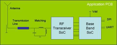
Figure 1: Application PCB with separate RF and BB SoCs discrete SMT matching components and antenna
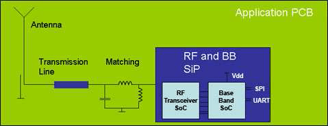
Figure 2: Application PCB with complete RF SiP and discrete antenna and matching network
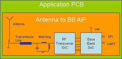
Figure 3: Application PCB with fully integrated Antenna in Package
Antenna in Package Design Methodology
The design methodology (summarized in Figure 4) developed at Insight SiP for RF SiP modules uses a combination of circuit and electromagnetic simulation tools to create a design progressively from basic schematic representation to a complete 3D electromagnetic representation of the layout.
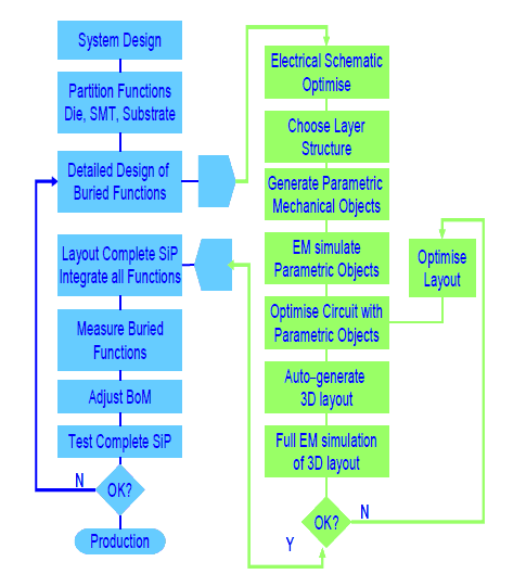
Figure 4: The methodology summary
The key to the success of this design flow is the use of progressively more accurate models of each part of the RF SiP as the design progresses from feasibility to production ready 3D layout.
Antenna Design
The design philosophy adopted for the antenna uses the same basic flow and tool-set in order to maintain optimum speed and precision throughout the AiP design process.
The key design constraints when designing an integrated antenna for an AiP module are:
‐ Miniaturization of the antenna to fit into a small footprint. Typically the antenna footprint target is a reduction of a factor of 2 to 3 compared to a discrete antenna.
‐ Adaptability of the antenna topology to be realized using the chosen SiP technology (organic or ceramic substrate or mix with IPD)
‐ Return loss over the operating bandwidth. This can be relative to 50 ohm or some other impedance chosen relative to the RF transceiver impedance
‐ Radiation efficiency to ensure minimum loss within the antenna structure
‐ Radiation pattern to match system and regulatory requirements
‐ Sufficient margin in terms of operating band to allow for the effects of ground plane size on antenna frequency tuning. Typically this needs to be at least 5% more than the operating band for 2.4 GHz ISM band antennas.
The Antenna in Package approach described here offers a simple solution path for system integrators that eliminates the need for costly and time-consuming detail RF design at the application level.
__________________________________________________________________
This is a guest post by Insight SiP which is a fabless RF system-in-package (SiP)