

ICsense
Belgium
ICsense offers mixed-signal IC design and ASIC supply services for the automotive/aerospace, industrial, consumer and medical markets. The company is ISO9001:2008 and ISO13485 certified with design HQ in Belgium and sales in Japan, U.S. and Germany
Services
ASIC design and supply
ICsense offers a broad range of ASIC development services; from ASIC design to delivering one-stop-shop ASIC solutions including
- study
- design
- packaging
- bench test
- production (ATE) test
- characterization
- qualification
- SCM (Supply Chain Management)
In close cooperation, ICsense custom develops the ASIC according to your requirements. As a one-stop-shop for ASIC design and supply ICsense will lead you from the initial business case to the delivery of your final ASICs in mass production.

This makes ICsense stand out:
- One-stop-shop for ASIC design and supply
- Short time to market
- System-level involvement and commitment
- ASIC tailored to your application
- Broad IP portfolio
IC design services
ICsense’s expertise is in analog, mixed-signal and high-voltage IC design with a focus on:
- High-performance and low-power
- Power and battery management
- Sensor, actuator and MEMS interfacing/acquisition
- High-voltage IC design
DESIGN & LAYOUT SERVICE
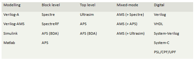
- Industry standard tools: Cadence, Synopsys, BDA, …
- Modelling in Verilog-A, VHDL-AMS, Verilog-AMS
- Design of advanced analog, mixed-signal, high-voltage integrated circuits
- Design for testability (DFT)
- Full PVT (process voltage temperature) and Monte Carlo simulations
- Layout service
- Digital design, VHDL coding
PROTOTYPING SERVICE
- Managing the manufacturing, (ATE) test, and packaging process
- Bench-testing and characterization of the developed prototype
- Fully-equipped in-house measurement lab
- Temperature forcing equipment Thermonics T-2800
INDUSTRY-STANDARD EDA TOOLS
ICsense has developed a unique design environment for high-quality analog and digital design in a structured way, resulting in a high reliability and high first-time-right success rate.
STRUCTURED DESIGN METHODOLOGY
Key benefits:
- Structured and formalized design approach using design plans
- Traceability of design choices and trade-offs through version control and design plans
- Reliability of results by full mixed-signal simulation coverage and reporting
- Extensive digital simulation coverage and constraint randomized verification
Key Features:
- Top-down, bottom-up design methodology
- Automated characterization over corners, supply and temperature
- Powerful simulation result and corner data processing
- Technology-independent platform
- Simulator-independent platform
- Embeds design plans for most analog blocks e.g. amplifier topologies, low dropout regulators, oscillators, bandgap references, temperature sensors, …
- Code, condition, functional and assertion coverage in digital simulation
- Version control (Cliosoft)
- Issue management (JIRA)
PROPRIETARY DESIGN TOOLBOXES
- DC-DC converters (inductive and capacitive / buck, boost, buck-boost, flyback)
- Delta-sigma analog-to-digital converters
- SAR analog-to-digital converters
- Pipelined analog-to-digital converters
- Delta-Sigma fractional-N synthesizers
- Digital-to-analog converters
- Phase-locked loops (PLL)

ASIC business case validation
- Feasibility study and concept definition
- Optimal choice of architecture and circuits
- Choice of technology and package
- Power, area, yield estimates
- Cost, timing and risk assessment
Sensor/MEMS interfacing
ICsense offers expertise in the following areas:
- MEMS interfacing
- Resistive sensor interfaces: Wheatstone bridge readout
- Capacitive sensor interfaces: tilt, accelerometer, pressure sensors, …
- Magnetic sensor interfaces: Hall sensors, GMR (giant magneto resistance) sensor interface
- Inductive proximity sensors
- High accuracy, fully integrated temperature sensors
- Delta-Sigma (ΔΣ) analog-to-digital (AD) converters: continuous and discrete time
- Successive approximation AD converters
Power management
ICsense offers expertise in the following areas:
- LDO regulators: low quiescent current / high current output
- Protection circuits: current, voltage and temperature overprotection
- Integrated switching-mode power supplies (highly-efficient DC-DC converters):
- Buck, boost, buck/boost, fly-back, … topologies
- Continuous and discontinuous
- Voltage and current mode
- Single phase or multiphase
- High-frequency – small inductance
- Asynchronous and synchronous
- Pulse width modulation (PWM) – Pulse frequency modulation (PFM)
- Integrated charge pumps and voltage doublers
- Wireless charging and battery management: state-of-charge, state-of-health
High-Performance and low power
ICsense offers expertise in the following areas:
- Bandgap references: low-voltage (LV) and high-voltage (HV)
- Instrumentation amplifiers: chopping amplifiers
- Low drop out (LDO) regulators
- Low-noise switched capacitor circuits
- Low-noise correlated double sampling (CDS) sample & holds
- Operational transconductance amplifiers (OTAs): offset compensation
- Phase-locked loops (PLL): low jitter, delta-sigma fractional-N synthesis
- Reference buffers
- High-precision, temperature-stable Xtal-less oscillators
- Digital-to-analog (DA) converters: high-accuracy, high-yield, fast-settling
- Delta-Sigma (ΔΣ) analog-to-digital (AD) converters: continuous and discrete time
- Successive approximation AD converters
- Pipeline AD converters
- Inductive bi-directional low-datarate link
- Monolithic oscillators with low-phase noise
- Ultralow-power circuits
High-voltage design
ICsense offers expertise in the following areas:
- High-voltage (bi-directional) switches
- High-voltage I/O buffers
- Class AB/G/H amplifiers
- Class D audio amplifiers
- (Self-oscillating) power amplifiers
- High-voltage low drop out (LDO) regulators and bandgap references
- High-voltage DC-DC converters: capacitive and inductive, buck, boost, buck-boost, flyback, converters and controllers
- High-voltage charge pumps and voltage doublers
- High-voltage instrumentation front-ends
- H-bridge (e.g. motor steering applications)
- MEMS and piezo drivers (ultrasound)
- High-voltage drivers:
- MEMS drivers
- Line drivers
- Gate drivers
- Laser/LED/LCD/backlight drivers
- Low-side (LS) and high-side (HS) drivers
- Electrode-array drivers (brain, nerve interfaces)
- Solenoid (coil) driver
Test and packaging
ICsense is an experienced partner in delivering the right ATE HW/SW solution and package for your IC.
Test solutions:
- Fully equipped measurement lab for ATE test correlation and bench testing
- Thermostreamer Thermonics T-2800 for bench characterization
- Access to ATE platforms such as: Teradyne uFlex (+DC90 module), Credence D10 and more
Assembly/packaging:
ICsense cooperates with world leading packaging centers to provide the IC package you request. During an ASIC development traject, the various packaging options are compared (technical/cost)
Most common packages include: QFN, BGA, ceramic, …
ICsense has built up considerable expertise in flip-chip and WLP (Wafer Level Packaging) solutions to accommodate for lowest form factor and highest performance.
Alternatively, ICsense can deliver bare dies in various forms (blue foil, waffle packs, …)
Industrialisation
ICsense lead the industrialization phase to deliver well-established ASICs in your target volumes, ranging from a few 100k/year to multi-million units/quarter. Early in the design process, ICsense takes DfM (Design for Manufacturing) and DfT (Design for Test) already into account.
A Single Layer Maskset (SLM) is generated to start volume production. The ASIC is first qualified by means of an industrialization lot (of a few batches) and a skew lot in most cases. From the devices in the industrialization lot, ICsense collects statistical data and freezes the production test (ATE) limits. The skew lot is processed to prove the robustness of the ASIC over process variations, and to ensure high yield.
Qualification is done on the final devices before SOP (Start Of production). Typical qualification levels are:
- JESD47G (Industrial)
- AEC-Q100 (Automotive)
Extra qualification tests can be carried out depending on the specific environmental operating conditions of the ASIC (“the mission profile”), and/or specific customer requests to ensure long-term ASIC compliance in the field.
Supply Chain Management
ICsense provides full supply chain management, from taking in orders from customers, over managing manufacturing subcontractors and continuous monitoring of product quality, to management of inventory and transportation of final goods to customer’s global warehouses.
ICsense controls the supply chain of your product from order to delivery on time at the location of your preferred manufacturing site. The SCM service includes:
- Wafer ordering and production follow-up
- Quality control
- Logistics/insurance optimisation
- Subcontractor management
- Cost optimization through test efficiency and yield management
- Customer return and FA (Failure Analysis)
What customers say:
“The wealth of knowledge and experience demonstrated by ICsense throughout a rather intense qualification process, provided us with the unwavering confidence that we have selected an ideal partner for our ASIC design needs,” said Yuval Cohen, Chief Technology Officer of Audio Pixels. “Additionally, ICsense’s turnkey approach which includes test and manufacturing services, delivers an efficient and cost effective mass-production solution to seamlessly integrate the High-Voltage ASIC driver with our MEMS structure.”
Functional safety
ICsense has a broad expertise in ASIC design for functional safety (e.g. SIL-3 qualification). On the website, business cases can be consulted in a variety of markets.
