Wireless Transceivers RF CMOS Front Ends
During the last decades, important advances in microelectronic techniques and technologies had been fueling the introduction of new wireless enabled products accessible to a large number of people around the world. Without the competitive price offered by CMOS, the widespread use of wireless enabled engineering complex devices, e.g. smartphones, tablets, etc. would certainly have been delayed. At the same time, these advances have been inspiring research and industrial institutions to develop the next generation of such products. Thanks to large efforts in research and development, the digital part of a radio transceiver has been growing to accommodate complex signal synthesizing as the ones necessary to transmit the constantly growing amount of data exchanged by the most recent wireless connected devices.
While advanced node CMOS processes have been helping to integrate systems on chip (SoC) hosting complex digital basebands, these processes had shown their limits to generate the analog signal to be radiated. The generation and radiation of this signal represent a lot of challenges. A large power level is required to guarantee a resilient and reliable connection between two devices, located from centimeters to kilometers away from one another. At the same time, this signal should not interfere or be interfered by any other, external or internal to the device. Furthermore, the generation of such a signal should be as efficient as possible to guarantee long battery lifetime for mobile or remote user convenience.
This paper provides an overview of the different wireless transceivers analog architectures and related radio frequency front end (RF FE) modules. It describes some of the challenges associated to the integration of the transceiver blocks in CMOS processes and provides a survey of the current efforts to address these challenges. It is structured as follows: after this short introduction, section II provides a short description of the most common analog architectures. Section III describes the challenges associated with the integration of the key blocks of the RF FE associated with each of these architectures and details some examples of successful implementations in different CMOS processes. Section IV provides some conclusions based on the previous sections.
ANALOG FRONT-END ARCHITECTURES
A radio transmitter generates a signal modulated by information to be transmitted. A radio receiver recovers and interprets this information after demodulation of the signal. Both blocks are part of a transceiver which have four complementary functions: signal modulation/demodulation, frequency translation (upconversion/ down-conversion), power amplification (high power/low noise) and radiation/ reception.
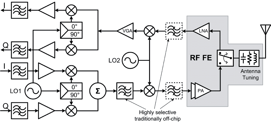
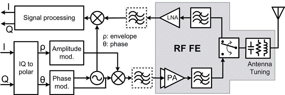
Fig. 1. Analog FE architectures: (a) Cartesian heterodyne, (b) Polar homodyne
There are two different transceiver analog architectures, see Fig. 1.a and 1.b. The first one, the heterodyne, is more robust to interference thanks, in part, to a simple or double intermediate frequency ( fI ) translation stage. The second one, the homodyne, has no fI stage making it more susceptible to interference and other issues, but easier to integrate. In modern wireless devices such as mobile phones, many radio transceivers should coexist for each specific communication standard. Homodyne architecture is therefore preferred due to its reduced die area and low off-chip passive element count (e.g. SAW filters).
Depending on the way the transmitted/received signal is synthesized/decomposed, homodyne architectures could be Cartesian or polar. If the signal is synthesized/decomposed from/to the in-phase (I) and quadrature-phase (Q) baseband information, the architecture is Cartesian (Fig. 1.a) and it is polar if the signal is synthesized/decomposed from/to the envelope and phase information (Fig. 1.b). Even though the polar architecture needs extra digital blocks, recently it has been gaining a lot of momentum among industrial and research institutions, thanks mainly to the fact that many of the signal emission/reception constraints rely on the digital blocks and not on the RF ones which become therefore easier to integrate. The following section describes some of the challenges of integration of the key RF blocks of modern wireless transceivers.
CMOS RF FRONT-END
In order to optimize power consumption, reduce area and costs, the ultimate goal is to integrate the whole transceiver, including its RF front end elements. On the receiver side, after a frequency band filtering the signal should be amplified in order to allow the following blocks extract the embedded data without or with little error. The amplification stage (low noise amplifier, LNA) should therefore add as low noise as possible to the received signal. Being, that noise is mainly a function of the LNA’s active elements, a reduced transistor noise figure will relax design constraints. Fig. 2 shows the 1/f noise of two identical size transistors, fabricated using the Altis ATS-130RF process, one with a low noise extra process mask and the other one, without it. From this figure, it is easy to understand the advantage of using the first device for LNA design. A largely successful receiver module integrated in top-selling 3G/3G+ mobile phones was designed using this extra process mask. LNA noise figure was reduced by up to 1.2dB with a minor gain penalty of 0.5dB. Low noise transistors are a good support to design, for among others, low noise phase locked loops (PLL) for large band frequency synthesizers required in modern wireless transceivers. Mobile phones, tablets and others should receive/transmit data/ voice at different frequencies under multiple standards: GSM, WCDMA, LTE, Wi-Fi, Bluetooth, NFC, GPS, etc.
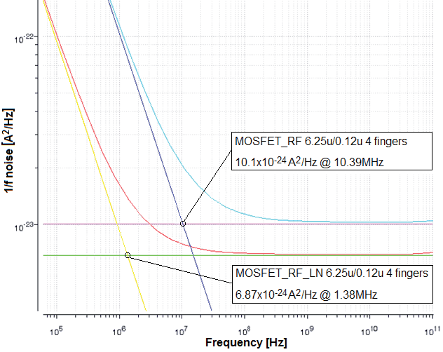
Fig. 2. Flicker noise minimization
On the transmitter side, a lot of efforts have been allocated to the power amplifier (PA) integration. As CMOS process node shrinks, voltage supply values decrease making it more difficult
for an integrated solution to generate the large amount of power required. This issue is stressed by the lack of active devices able to handle the large values of voltage swing typical of PA
output stages. Furthermore, since the PA module demands a large amount of current from the battery of a mobile device, power level conversion efficiency is a key factor for long
battery autonomy. The larger amount of leakage, lower voltage supply and the lack of high voltage robust active devices in deep submicron compared to 130nm and/or 180nm CMOS
processes make the last ones more suited for PA integration. The same is true for the very last stages of the transmitter RF front end: the switch and the antenna tuning.
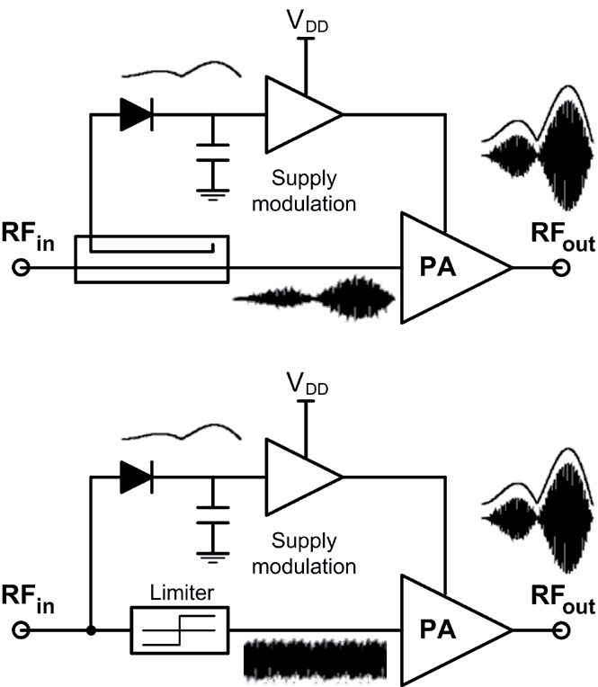
Fig. 3. RF front end (a) ET and (b) EER topologies
Modern wireless communication standards aim to allow transmitting a large amount of data modulated in complex signal waveforms. A highly linear amplification stage is required to minimize the amount of distortion. Highly linear PAs are less efficient than nonlinear ones; nevertheless some techniques help to partly overcome the nonlinearity while keeping high efficiency levels. Meant to be integrated with polar architectures, envelope tracking (ET), see Fig. 3.a, and envelope elimination and restoration (EER), see Fig. 3.b, are two RF front ends topologies helping minimize the distortion
introduced by highly efficient nonlinear PAs. In both, the information contained in the envelope of the signal is sampled (ET) or extracted (EER) before amplification and reintroduced by PA supply modulation. In ET topology the signal is amplified by a nonlinear PA (e.g. deep class AB) while in EER topology the signal from which envelope information has been removed, could be amplified by switch-mode PAs. Switch-mode PAs could theoretically attain an efficiency of 100% but in practice this efficiency ranges up to 40-50% [1], [2]. Deep class AB PAs have typically efficiencies ranging up to 30-40% [2], [3].
At the last stage of the RF transmitter, after the PA module and before the antenna filter, a switch is required to commute between the receiver and transmitter paths. This switch should be able to withstand the large voltage swing generated by the PA remaining highly linear and adding low noise. Between the antenna and the switch, an antenna tuning module is suitable to minimize the power loss due to antenna mismatching. PA, antenna switch and antenna tuning have remained three separate module chips in most of the modern transceivers. Furthermore, their requirements from a technology process point of view differs from one another. For PA integration, the most important features are low leakage, low parasitic fast enough RF transistors able to sustain a large enough voltage swing together with good quality passive elements (inductors, capacitors, resistors). For switch integration, the main process figure of merit (FOM) is the RONCOFF of the active devices. For
antenna tuning integration, the most important parameters are the RON and the linearity of the active devices and substrate, together with good quality capacitors of different capacitance density. A few companies have introduced pure CMOS PA modules for the wireless mobile devices market [4], [5] with moderate success. None offered switch and/or antenna tuning pure CMOS modules. While most of the three modules are designed and fabricated in compound processes such as GaAs or SiGe BiCMOS, a promising solution is gaining a lot of attention recently, CMOS silicon on insulator (SOI). Innovative solutions integrated in CMOS-SOI, as the one recently introduced by a major integrated wireless communication solutions provider [6] offer highly integrated modular RF front
ends, customizable by the world region. While this solution remains modular it represents a big step in the development of fully integrated, RF FE included, CMOS transceivers.
CONCLUSIONS
From what has been exposed, a high degree of process customization and optimization is required to help design and integrate the different blocks of modern CMOS RF front ends. Specialty foundries, facilitating this customization and optimization, help develop the next generation of transceivers. By accompanying innovative small, medium and large RF solution providers from the specification of their technical needs to the final production, specialty foundries provide what is frequently off-reach for large foundry providers; a co-design circuit-process, essential to achieve high integration levels,
allowing offering the latest technical developments to a large public in an affordable way.
REFERENCES
[1] A. Grebennikov, N. O. Sokal, M. J. Franco “Switchmode RF and Microwave Power Amplifiers,” 2nd ed., Academic Press 2012.
[2] S. C. Cripps, RF Power Amplifiers for Wireless Communications, 2nd ed., Artech House, 2006.
[3] B. Kim et al., “Envelope tracking technique for multimode PA operation,” EU Microwave Conf. 2009 proc., pp. 429–432.
[4] “AX508 GSM/GPRS Quad Band Power Amplifier,” www.skyworksinc.com/ uploads/documents/ax508pb.pdf, 2009.
[5] “RFaxis Granted Four Fundamental Patents for Its Disruptive Single-Chip Single-Die RF Front-end Integrated Circuit (RFeIC) Technology” http://www.rfaxis.com/press/2012_1_26
[6] “Qualcomm RF360 Front End Solution,” http://www.qualcomm.com/media/ documents/files/qualcomm-rf360-front-end-solution-product-brief.pdf, July 2013.
___________________________________________________________________________
This is a guest post by Altis Semiconductor – which is a European based specialty foundry.