

An Application Specific Integrated Circuit (ASIC) is a specialized integrated circuit crafted for a particular use or purpose. Typically, ASICs are tailored for products targeted for mass production, consolidating necessary electronics onto a single chip.

ASIC stands for “Application Specific Integrated Circuit.”
Despite the substantial initial design cost (known as NRE – non-recurring engineering costs), ASICs can prove cost-effective for high-volume applications. This is especially true when a significant portion of a system can be integrated into a single ASIC, reducing the need for external components. ASICs have played a pivotal role in technological advancement, shrinking the size of electronic devices and boosting logic gate density per chip. Examples of ASICs include Intel’s CPUs and Nvidia GPUs that includes both digital logic and analog components to create an entire design on a single chip.
There are two primary methods for custom ASIC design:
Semi-custom design itself is divided into few groups. The classification of ASICs is shown in the figure 1a below:
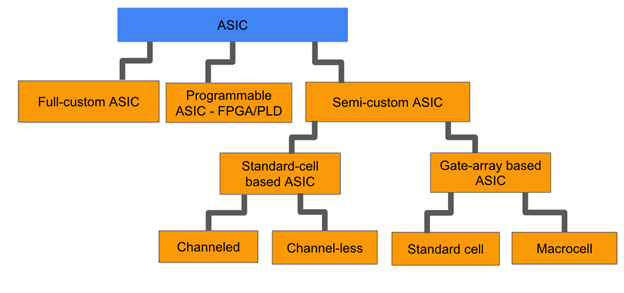
Figure 1a: Types of ASICs
Full custom ASIC design refers to the creation of a unique integrated circuit from scratch, tailored to meet specific requirements. This approach involves a high level of customization and offers the greatest level of control over the design process. With full custom design, every aspect of the ASIC, from the transistors to the interconnections, is explicitly defined by the ASIC engineer.
The journey of designing an ASIC is a long winding road which takes you from a concept to a working silicon. Although the end product is typically extremely small (in mm2), the journey is quite interesting, full of challenges and trade-offs which the designers need to wrap their heads around to make the best engineering call. This post covers the different steps in the ASIC design starting from ASIC design specification to design tape-out for manufacturing in the foundry, packaging and testing and highlight important decisions and activities that each step entails.
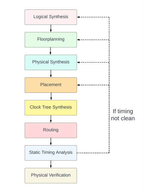
Figure 1b shows the flow chart for the ASIC design from design to chips.
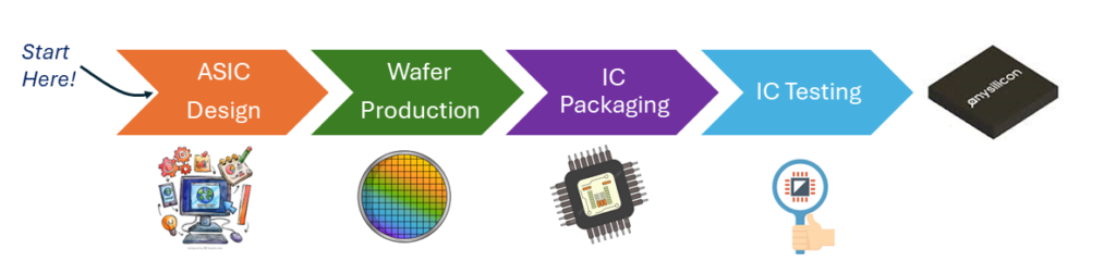
Figure 1b: ASIC Design from Spec to Chips
ASIC Design: This step involves conceptualizing, specifying, and implementing the functionality of the ASIC using RTL design, hardware description languages (HDL) like Verilog or VHDL, followed by design verification to ensure correctness. At the end of this step, a GDSII file will be sent to the foundry. The design is done using Electronic Design Automation tools (EDA).
Wafer Production: After finalizing the design, the ASIC layout data is used in the semiconductor fabrication process, involving steps such as photolithography, etching, doping, and metallization to create the integrated circuit on silicon wafers.
IC Packaging: Once the wafers are processed, individual ASIC dies are cut and packaged into their final forms, which involves encapsulating the die in a protective package and connecting it to external pins or leads for integration into a PCB.
IC Testing: Packaged ASICs undergo electrical testing to ensure they meet quality and performance requirements. This includes functional testing to verify correct operation and parametric testing to validate electrical characteristics, ensuring only high-quality ICs are delivered to customers. Typically done in automated test equipment (ATE).
Get a fast indicative cost range, then unlock a full breakdown by email.
IP cores, or intellectual property cores, play a significant role in ASIC design. They are pre-designed and pre-verified blocks of reusable hardware or software components that can be integrated into the overall design.
When it comes to intellectual property cores, there are typically three options for ASIC designers:
Chip design teams play a crucial role in ASIC design. These ASIC engineers are responsible for the design effort of designing, implementing, and verifying the overall chip design (digital circuit, memory blocks, analog circuits etc.). A typical ASIC engineering team consists of various members with specialized roles and expertise with electrical engineering background.
EDA (Electronic Design Automation) tools are computer-aided design tools that are crucial in Development process, aiding ASIC designers at various stages of the process. These third-party design tools streamline design, enhance productivity, and ensure accuracy. Common ASIC design tools include logic design (e.g., Cadence Design Systems’ Genus, Mentor Graphics’ Questa, Synopsys’ Design Compiler), simulation (e.g., Mentor Graphics’ ModelSim, Cadence Design Systems’ Xcelium, Synopsys’ VCS), and logic synthesis tools.
The first step in ASIC design flow is defining the specifications of the product before we embark on designing it. This phase typically involves market surveys with potential customers to figure out the needs and talking to the technology experts to gauge the future trends. The latter is particularly important because ASIC design cycle may be anywhere between 6 months to 2 years. It is therefore important to foresee and predict what trends would be relevant 1-2 years down the line if one needs to sell their product to a wide audience.
This marketing research translates into high-level product specifications like top-level functionality of what you intend to do with your ASIC, specific computation algorithm that you want to implement, clock frequencies that would make the product appealing to the customers, package type- Ball Grid Array (BGA) or CSP (Chip Scale Package) etc., power supply, communication protocols that will help interface with the external world, temperature range that you would want your product to work in.
Developing a thorough and correct specification usually sets a solid foundation for the ASIC development. The technical specifications need refinement of the technical requirements over time, but it’s important to cover the information in an unambiguous manner.
In term of pricing, there is now sufficient information regarding the NRE (non-recurring engineering costs) and the component cost. The component cost is important because it translats directly to the potential revenue of the company.
After pruning the specifications, it’s now time to partition the entire ASIC or SOC’s functionality into multiple functional blocks using a block diagram. Architects like to brainstorm many possible options for the architecture and discuss their pros and cons while considering- performance implications, technical feasibility, and resource allocation in terms of both cost and time. A good architecture focuses on gleaning the best electrical performance of the ASIC chip, while minimizing the hardware resources which directly helps in keeping the overall cost of the chip within the allocated budget. During this architectural design, chips engineers define the relationship between various functional blocks and allocate time budget to each block. All these technical details are captured in an architecture document that includes a high-level block diagram for the entire design (single chip) and detailed block diagrams for each functional block.
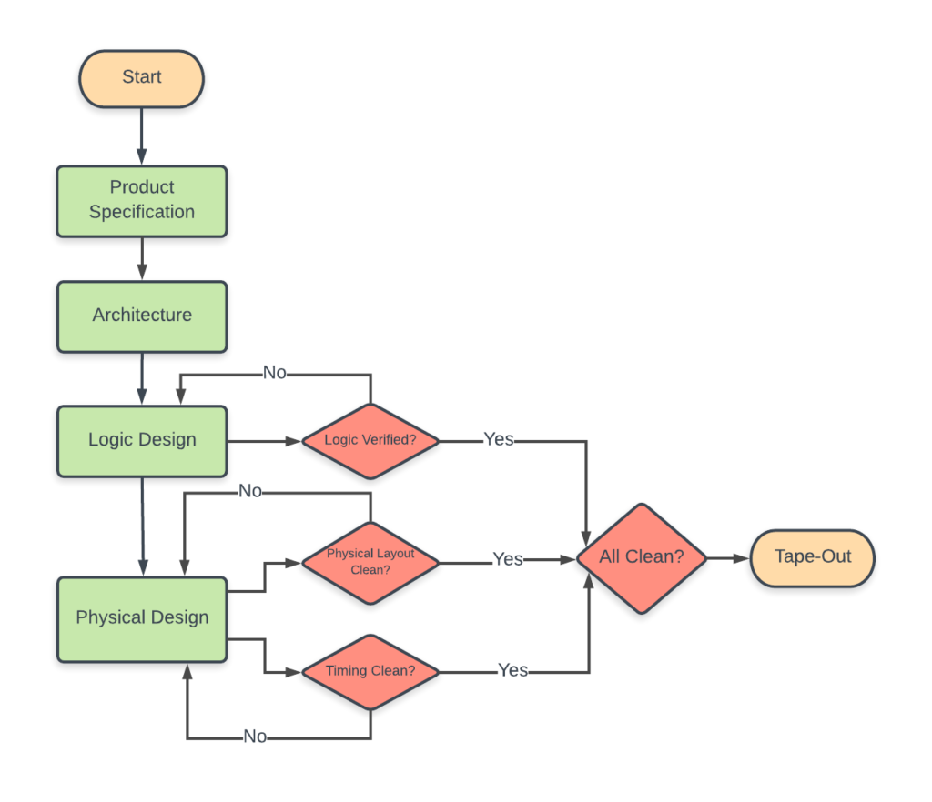
Figure 2: ASIC Design Flow
Once you have high-level idea of all the functional blocks needed, it would be prudent to identify the critical modules and possibly brainstorm whether you need to re-use those IPs from previous projects, make necessary changes to the existing IPs or perhaps procure them from other parties.
The divide between hardware and software blocks is also a critical part of this phase of the ASIC design. Design is captured in a high-level programming language like C++ or System C.
This step refers to the front-end part of the ASIC design flow and involves coding the data flow of each functional block in a hardware description language like Verilog, VHDL or System Verilog. The interactions between the functional blocks are also coded. Logic Design usually comprises of:
Combinational Logic: Combinational logic usually refers to Boolean combinatorial gates like the OR, AND, NAND, NOR etc. While these gates are simple, these can be combined to perform complex digital logic operations.
Finite State Machines (FSMs): These are higher abstractions of sequential logic which can be implemented both in hardware and software. FSMs model the response of a digital machine to a set of inputs to produce a deterministic set of outputs, and serve as an important building block for logic designers.
Arithmetic Logic Blocks: Arithmetic computations form the heart of the computing digital circuits and are crucial for performance in high-performance CPU cores. Arithmetic computation includes addition, subtraction, multiplication, and division. There are numerous possible implementations of these circuits which offer a trade-off between performance, area, and power. Logic designers can choose one best suited for their application to optimize for one or more parameters.
Data-path Design: In addition to coding combinations of above elements, Hardware Description Languages (HDLs) can model data path design in an abstract manner like a programming language which can be interpreted by EDA tools correctly. These could be multiplexing, decoding, case statements etc.
This step is also called ASIC front-end design.
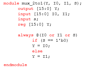
Example of a behavioral HDL code for 2:1 Multiplexer:
In parallel to logic design, the verification team needs to develop a verification plan for both digital and analog logic components and create a testbench to be able to test the design for all possible corner cases to ensure correct functionality which needs to be consistent with the specification. This is required to perform a full functional verification of the chip. Writing the RTL usually takes around 10-20% of the entire design cycle time, while Verification accounts for 80-90% of the time. ASIC verification will also include formal verification.
This refers to the backend design cycle. Sometimes called: design implementation. If there’s just one aspect that distinguishes the backend design from frontend design, then it would be- delay. Frontend design, while being cognizant of the logic delays and speed, largely ignores it for the majority part of the RTL coding (RTL design) and verification. While, on the other hand, physical design sees real delay right from the very beginning.
Physical design process is further sub-divided into the following:
Synthesis reads in the RTL code (.v or .sv files) along with physical libraries of the standard cells that may contain- delay information (.lib files), physical dimensions, and metal layer information within the cell (.lef files) and other constraint files to convert the behavioral or dataflow code into real physical standard cell gates. Note that there are many possible implementations for 2:1 Multiplexer, and Synthesis is responsible to do an educated trade-off with performance, power, and area to come up with the best implementation considering these constraints. As an example for the 2:1 Multiplexer, one possible implementation is below:
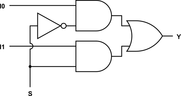
Figure 3: Gate level implementation of 2:1 Multiplexer
Floorplanning step formalizes and refines the floorplan that was first conjured up during the architecture planning step. In this step, the entire die area is divided into physical partitions, and their shapes are molded while keeping in mind the area requirements, the flow of top-level data and control buses, and the possibility of any future growth. Pins and ports are assigned a rough location, which can further be refined depending on the Place and Route results.
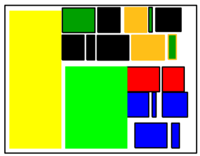
Figure 4: Floorplanning the blocks relative to each other. Image Courtesy: Andrew Kahng, UCSD
It’s quite common for physical design engineers to work on more than 1 floorplan in parallel, and try to evaluate which one works best for overall design QoR (Quality of Results). This is usually the most critical step in the physical design cycle and requires multiple iterations. Any additional time spent here is worth it considering its long-lasting implications on routing congestion, cell density, timing QoR, and DRCs.
A robust power grid delivery- which addresses static and dynamic IR drop is also a critical function of the floorplanning step.
During placement, all standard cells are placed in legal locations on site rows. The aim of this step is to minimize the wire length, while ensuring optimal placement that will help faster timing convergence. Memory blocks are also inserted in this design phase.
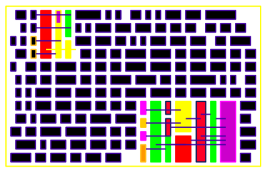
Figure 5: Standard Cells arranged on site rows. Image Courtesy: Andrew Kahng, UCSD
No real routes are laid during this step. Placement estimates routing through a step called Global Routing, where it estimates the total wire length and global route congestion. Many modern placement engines have the capability to take into account the switching activity from SAIF or VCD files, and try to optimize placement for achieving lower dynamic power.
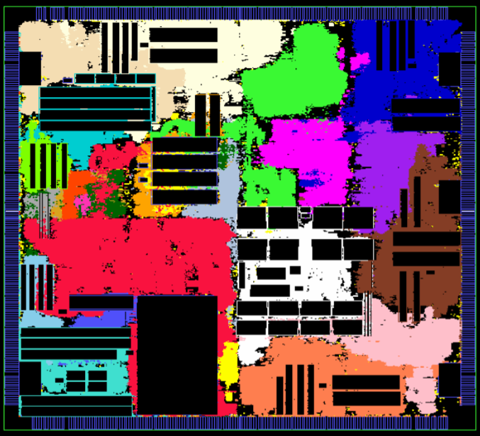
Figure 6: Placed design. Image courtesy: Andrew Kahng, UCSD
Till now, the clock network was ideal. During clock tree synthesis, clocks are propagated and the clock tree is synthesized using clock buffers. The major goals of this step are to achieve optimal clock latency while minimizing clock skew. There are many proposed algorithms to design an optimal clock tree- H Tree, Steiner Tree etc. In addition to this, one may choose Clock Tree Mesh, Multi-source Clock Tree Synthesis or traditional Single Point Clock Tree Synthesis which offer trade-offs for dynamic power, routing resources and OCV adjustment due to the common clock path.
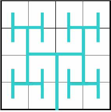
Figure 7: Typical H tree clock distribution. Image Courtesy: Research Gate
Clock being the signal with the highest toggling frequency in the design, the clock buffer tree accounts for over 75% of the dynamic power dissipated in an ASIC. The architecture may support clock gating to turn off idle parts of the chip to save dynamic power.
With all instances placed and clocks routed, now it’s time to route the signal nets. Modern process supports 10-12 metal layer stack, with M0-M1 reserved for standard cell routing. The algorithm used for detail routing is usually a glorified maze router with added constraints to ensure faster run-times. The metal resources are divided into tracks which are the legal locations for metal routes. The aim of detail routing is to ensure minimum detours because these may have implications on timing, and to ensure minimum DRC (Design Rule Check) violations like opens, shorts etc. This step performs multiple search and repair loops (10-20) to keep the overall DRC count low.
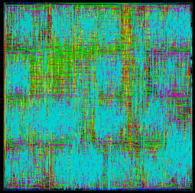
Figure 8: Routed Design. Image Courtesy: Andrew Kahng, UCSD
While logic verification ensures correct functionality, physical verification ensures correct layout. There’s been an increase in Physical Verification checks which includes- DRC (Design Rule Checks), LVS (Layout versus Schematic), Electromigration, Electro-static discharge violations (ESD), Antenna violations, Pattern Match (PM) violations, Shorts, Opens, Floating nets etc. It is important to track these violations in parallel with the Place and Route flow to avoid any surprises just days before tape-out.
Timing Verification verifies that the chip runs at the specified frequency by ensuring setup and hold are met for all timing paths in the design.
Figure 9: Chiplet ASIC Example
ASIC design flow is a complex engineering problem that goes through a plethora of steps from concept to silicon. While some steps are more like art than engineering (like floorplanning), others entail sound engineering trade-offs (like physical design and timing). With an increased demand for better performance and shrinking time to market, ASIC design process would continue to get more intricate over the next decade. The core motivation and design philosophy, however, would remain the same. This comprehensive approach ensures that the full potential of ASICs, including full custom ASICs, is realized in the realm of electronics and VLSI.
Some companies offer ASIC design as a service (e.g. ASIC design services or SoC design service), if you are interested in getting an offer from ASIC design service companies please click here.

Semiconductor foundries play a crucial role in the ASIC manufacturing process, as they are responsible for producing the custom-designed chips on silicon wafers. These Semiconductor foundries must have the capabilities and expertise to handle the complex photolithography, etching, and deposition steps involved in wafer fabrication. Selecting the right wafer foundry partner is essential for achieving the desired performance, power efficiency, and cost targets of the ASIC. Collaboration with a reputable foundry can help ensure the successful production of high-quality ASICs that meet the specifications and requirements of the design.
Once the design has been finalized and the GDSII file has been sent to the wafer foundry, the next step is the actual manufacturing of the ASIC chips on silicon wafers.
During the wafer production phase, the GDSII file is used to create a photomask, which is a template for the pattern that will be transferred onto the silicon wafer. The photomask is created using a process called photolithography, where ultraviolet light is used to selectively expose a photosensitive material on the wafer.
After the photomask is created, it is used to expose the silicon wafer multiple times, each time depositing a different layer of the ASIC design onto the wafer. This process involves several steps, including photomasking, etching, deposition, and polishing, to create the intricate layers of the semiconductor device.
Once the ASIC design has been fully fabricated on the wafer, it undergoes a series of inspections and tests to ensure its quality and functionality. This includes visual inspections, electrical testing, and functional testing. Any defects or abnormalities found during this process will require further investigation and potentially rework.
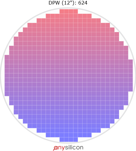
This Free Die per Wafer Calculator is a great way to start calculating your ASIC unit cost.
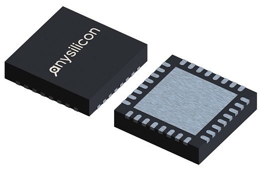
There are several types of packaging options available for ASICs, each serving different purposes and catering to specific needs. The choice of packaging can greatly impact the performance, reliability, and overall cost of the ASIC. Here are some common types of ASIC packaging:
Quad Flat Package (QFN)
The QFN (Quad Flat No-lead) package is probably the most popular semiconductor package today because of four reasons: low cost, small form factor and good electrical and thermal performance. In this article we will provide an overview to QFN packaging, discuss QFN package technical details and specifications in detail and present various versions of QFN package that are used in IC packaging.
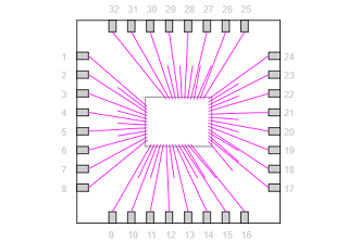
Wirebond diagram is an important setup in IC packaging, here is an example to QFN internal wiring. You can use this free Bonding Diagram tool to visualize your QFN internal wiring.
Ball Grid Array (BGA)
Ball Grid Array packages feature an array of solder balls on the underside of the package instead of leads. These solder balls make contact with corresponding pads on the PCB, enhancing thermal performance and reducing the risk of electrical interference. BGAs are widely used in modern electronics due to their compact size, excellent heat dissipation capabilities, and resistance to mechanical stress.

Chip-scale Packages (CSP)
Chip-scale packages are designed to be nearly the same size as the semiconductor chip they enclose, minimizing wasted space. CSPs are ideal for applications where size and weight constraints are critical, such as in mobile devices and wearables. They often use very fine-pitch solder balls or copper pillars for connections.
Wafer-level Packaging (WLP)
Wafer-level packaging is a technique where multiple semiconductor devices are packaged at the wafer level before they are diced into individual chips. This approach can reduce manufacturing costs and improve device performance. WLP allows for the creation of ultra-compact and high-density packages, making it suitable for applications like MEMS devices and sensors. Read more about wafer level packaging here.
Get a fast indicative cost range, then unlock a full breakdown by email.
What are the differences between ASIC and FPGA?
The design process for ASICs can take several months to a few years, while FPGAs are more flexible for prototyping and low-volume production. Ultimately, the choice between ASICs and FPGAs depends on the specific requirements of the project and the volume of production needed.
What is a full custom ASIC design?
A full custom ASIC design involves creating a custom integrated circuit, including logic gates, interconnects, and physical layout. The designer of a full custom design has complete control over the circuit architecture, optimizing it for performance, power, and area. The process begins with specification and high-level design, then detailed transistor-level circuit design. After designing the circuit, the physical layout is created, optimizing component placement. Interconnects are created to connect circuit components. The design is then sent for fabrication, where a silicon chip with the circuitry is created using photolithography, deposition, and etching.


