

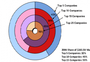
Vigorous M&A activity in 2015 and 2016 has reshaped the landscape of the semiconductor industry, with the top companies now controlling a much greater percentage of marketshare. Not including foundries, IC Insights forecasts to top five semiconductor suppliers—Intel, Samsung, Qualcomm, Broadcom, and SK Hynix— will account for 41% marketshare in
Read More
Let’s say you’ve got a great idea for a new musical Christmas card solution, and you go to a Big Foundry and a Big OSAT and convince them to supply you. Great. But let’s say there are several other musical Christmas card solution providers, and they’re also working with the
Read More
First off, we need to define what is meant by “quality” for this discussion. In generic terms it means something like “how well a product does its job”. For a chip, or a rather what comes out the end of a chip supply chain, this isn’t simply a measure of
Read More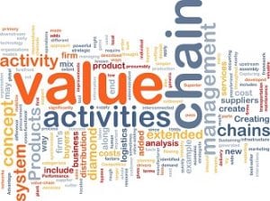
Michael Porter developed the value chain concept in 1980 in his book “Competitive Advantage”. A value chain is a series of activities within a company in order to deliver a product or a service. The total value delivered by the company is the sum total of the value built up
Read More
Each semiconductor company reaches at some point to the manufacturing dilemma – how to go into production in the cheapest, most efficient and highest quality way? Is it using an external full turnkey partner – e.g ASIC model, or work directly with semiconductor suppliers – e.g. COT model.
Read More

Allwinner Technology, a Chinese fabless semiconductor company that design and manufacture SoC processors announced a new laptop that could cost $79. Since its founding in 2007, Allwinner has released more than 15 SoC processors that have been widely implemented in Android-based tablets, as well as in smartphones, laptops and more.
Read More