We wrote before about multi project wafer benefits for IC designers of using MPW multi-project-wafer services.
Multi Project Wafer service is allowing companies to share the expensive mask cost. Essentially, Multi project wafer (MPW) services integrate onto silicon wafers several different integrated circuit designs from various teams. These designs are typically from companies, researchers and IP vendors that want to test their design at a lower cost.
As Maskset costs are extremely high (and only increasing), it makes sense to share mask and wafer resources to produce designs in low quantities.
As the costs of Maskset are exceedingly high and continually rising, it is logical to pool mask and wafer resources to manufacture designs in smaller quantities.
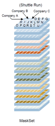
The following image describe the structure of an MPW wafer:
Presently, Multi Project wafer (MPW) services are available by all the leading semiconductor foundries and well as their channel partners. Multi Project Wafer is considered as a business enable to the foundry market. This means that the MPW service is helping the foundries grow their business.
Multi-Project Wafer (MPW) services are used to fabricate multiple integrated circuit (IC) designs from different customers on a single silicon wafer. This is a cost-effective way for smaller-scale projects or research efforts to access semiconductor fabrication facilities without bearing the full cost of manufacturing an entire wafer for their own design.
Here’s how the MPW process typically works in terms of placing dies on a MPW wafer:
Design Submission: Customers submit their designs to the MPW service provider. These designs are often in the form of GDSII files, which contain the layout information for the integrated circuits.
Design Compilation: The MPW service provider compiles all the submitted designs into a single reticle. A reticle is essentially a mask used in photolithography to transfer the circuit patterns onto the silicon wafer. The compilation process involves arranging the different designs on the reticle in such a way that they fit together efficiently while adhering to design rules and minimizing wasted space.
MPW Reticle Mask Creation: Once the compilation is complete, the reticle mask is created. This involves using a photomask fabrication process to transfer the circuit patterns from the digital design files onto a physical mask. The mask will be used during the lithography step of the wafer manufacturing process.
MPW Wafer Preparation: A silicon wafer is prepared for the manufacturing process. This means cleaning the wafer to remove any contaminants and preparing the surface for the deposition and etching steps.
Lithography: The reticle mask is used in the lithography step to transfer the circuit patterns onto the silicon wafer.
Etching and Deposition: After lithography, the wafer undergoes a series of etching and deposition steps to create the actual circuit structures. Etching removes material from the wafer where it is not protected by the hardened photoresist, while deposition adds material to build up the desired circuit features.
Die Separation: Once all the circuit structures have been fabricated on the wafer, the individual dies are separated from each other and sent to end customers.
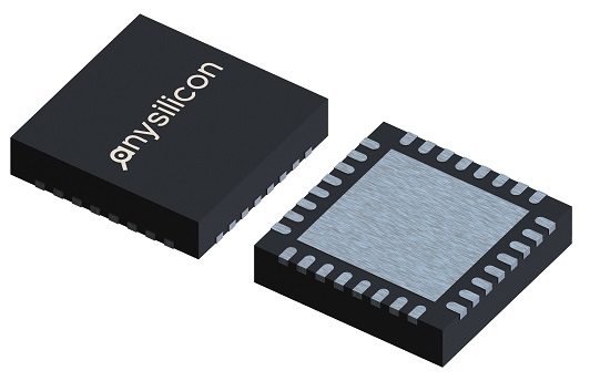
Different types of packages can be used on MPW runs depending on the specific requirements and the type of integrated circuits manufactured. A few types of packages are very common in the industry: ceramic packaging, plastic packaging, chip-scale packaging materials (CSPs) or quad-flat no-lead (QFN) packaging and more. Get a price for your IC package here.