

Clock Gating is defined as: “Clock gating is a technique/methodology to turn off the clock to certain parts of the digital design when not needed”.
With most of the SoCs heavily constrained by power budgets, it is of utmost importance to reduce power consumption as much as possible and clock gating is one of the simplest and most used method to reduce the dynamic power of the design. The concept is simple. Turn off the design when not needed – without effecting the functionality. By turning off the clock to the design/system, essentially the switching activity of the design is reduced and thus dynamic power. Clock gating can be applied to smallest part of digital design (a single FF) up to complete subsystems or entire SoCs.
Generally, there are two different techniques of implementing clock gating.
We will only focus on first type of Clock gating here. Normally, complete clock gating strategy is defined in the architecture of the system and then designers implement that strategy. There are different techniques to implement the clock gating.
In simplest form a clock gating can be achieved by using an AND gate as shown in picture below
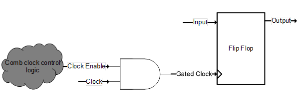
Figure 1: AND gate-based clock gating
The clock enable signal, generated by a combinatorial logic, controls when to provide the clock to the downstream logic (FF in the above figure). When enable is 1, the clock will be provided to FF and when enable is 0, the clock will be turned off and thus FF will not be active.
However, this simplest form of clock gating technique has some problem of generating glitches in the clock provide to the FF, which are not desirable.
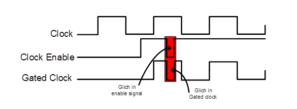
Figure 2: Glitches in enable/gated clock
These glitches can be removed by introducing a negative edge triggered FF (assuming downstream FFs are positive edge) or low-level sensitive latch at the output of the clock enable signal.
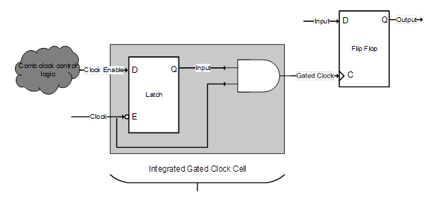
Figure 3: Latch based clock gating
This will make sure that any glitch in the clock enable signal will not be visible to the gated clock output. The Latch output will only be updated during the negative clock cycle and thus input to AND gate will be stable high.
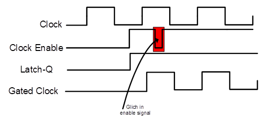
Figure 4: Glitch Free Gated Clock
When implementing such design, one can instantiate two separate cells from the library (latch and logical AND standard cells) or use one integrated clock gating cell from the library. These Integrated Gated Clock Cells are provided in every technology library for designers to use with an enable input signal, an ungated input clock signal and a gated output clock signal.
The clock enable signal can either be SW controlled or HW controlled. In case of SW controlled, the design is enabled/disabled by SW. In case of HW controlled clock enable signal, the control of gated clock is dynamically controlled by HW when needed. For example, a simple way to control the triggering of FFs is by using an XOR gate with inputs of XOR gate connected to input and output of a FF. If input and output of a FF are same in any cycle, the FF does not need to be triggered and thus clock will be gated (clock enable signal will be 0 ) and if they are different, clock enable signal will be 1 and thus clock will be provided to the FF.
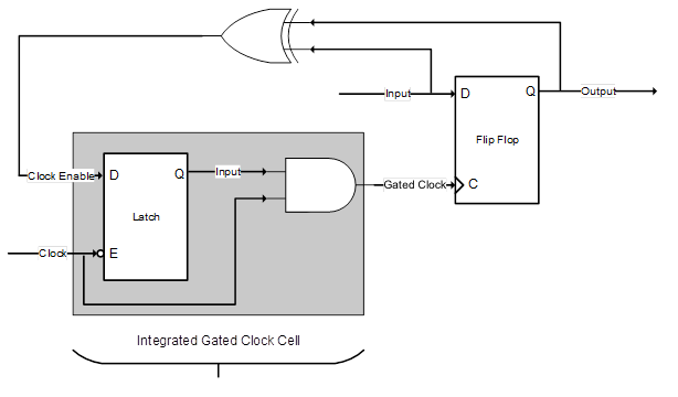
Figure 5: XOR based Clock Enable signal
The XOR feedback path can be combined with other clock enabling logic as well such as global clock enable signal. This will allow design to have clock gating strategy at multiple levels (from complete SoC level right down to a single FF).
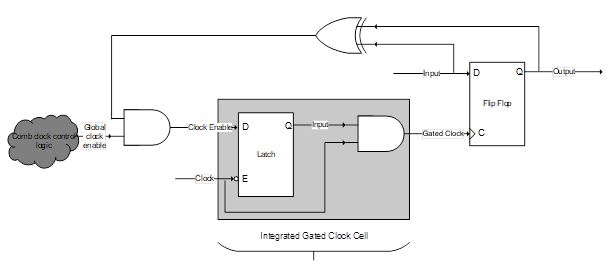
Figure 6: Clock gating with global enable signal
Also introducing the clock gating into the system, does introduce the physical gates into the clock paths as shown in above figures which will introduce clock skews between FFs and thus impacts setup and hold timings. These impacts must be compensated during clock tree synthesis to minimize the skews and balance the clock paths to all parts of design even with clock gating cells. One must be aware that increasing clock gating comes at an added cost of area. However, increase in area due to clock gating cells is normally very small as compared to power savings one can make.
In addition to above type of clock gating, there is sequential clock gating which involves a deep analysis of the design over several clock periods. Trying to do sequential clock gating manually is time consuming as it requires tracking of data over multiple cycles over several nodes of the design. The basic idea is simple. If a register X is not updated in cycle C, and is feeding a register Y in clock cycle C+1, then register Y does not need to be clocked in cycle C+1 since it already has correct value from previous cycle.
It should be highlighted that power and clock gating are two different techniques to reduce the overall power consumption within the SoC/ASIC. While clock gating focuses on the dynamic power of the circuit by reducing the switching frequency, the power gating focuses on the static/leakage power of the circuit by reducing the flow of current through the circuit.
The goal in power gating is to switch off the entire circuit when not in use. However, system that implement power gating, might need some extra functionality (such as retention flops) to retain the state and information during power down mode. Similarly, one might need to isolate powered down part of design with power ON design with isolation cells.
Power gating has become very common in lower (smaller) technology node circuits as static power has become more of an issue with reduced gate lengths.
What is clock gating cell?
It’s a one of clock gating technique that is based on instantiating two separate cells from a library: a latch and a logical AND standard cells.
What is power gating and clock gating?
Power and clock gating are two different techniques to reduce the overall power consumption within the SoC/ASIC. While clock gating focuses on the dynamic power of the circuit by reducing the switching frequency, the power gating focuses on the static/leakage power of the circuit by reducing the flow of current through the circuit.
Looking for prices?
Calculate your die per wafer (DPW)
Start your SoC design today, click here


