

PLLs (phase-locked loops) are common analog circuits in SOCs (systems on chips). Almost all SOCs with a clock rate greater than 30 MHz use a PLL for frequency synthesis. However, a “one-size-fits-all” PLL does not exist. The devices have a range of frequency, power, area, performance, and functions. PLLs implemented in 100 nm or smaller processes typically range in frequency from 10 MHz to 10 GHz. Their power spans from less than 1 mW to more than 100 mW. Their size can vary from 0.04 to 2 mm2, and their performance, which you typically measure as output jitter, ranges from more than 100 fsec to more than 10 psec.
The wide range of specifications is the result of the wide range of end uses. Some uses include digital-logic or processor clocking, analog-front-end ADC/DAC clocking, serial-link communication, and RF synthesis. This article focuses on frequency-multiplication PLLs, but many other types exist.
Period and long-term jitter
There are many reasons for the difference in power and area among PLLs. The most common reason is the jitter performance, although other requirements, such as output frequency and loop bandwidth, also contribute. Designers should primarily focus on period jitter and long-term jitter. Period jitter is the error that occurs when the output clock itself is acting as the trigger. In this case, you measure jitter at a hold-off time of one output period. In other words, it is the error—that is, phase error—of one clock period. You usually measure period jitter over a large number of samples of the output clock, and you can describe it using a peak-to-peak or an rms (root-mean-square) number.
The period jitter is of concern for static-timing analysis in digital circuits. For example, clocking a digital core at 1 GHz requires a nominal period of 1 nsec. However, no matter how good the PLL is, only the average period is 1 nsec. For static-timing analysis, you must know the shortest period to calculate timing margin. A high-quality PLL has period jitter on the order of 100 fsec for a 1-GHz output. This jitter consumes 0.01% of the output period—orders of magnitude smaller than the uncertainty in static-timing analysis. A PLL with minimal power consumption and area has period jitter on the order of 1 to 10 psec and consumes 0.1 to 1% of the output period, which is usually acceptable.
Long-term, or N-cycle, jitter is the measure of how much the PLL’s output-clock edge deviates from the position of an ideal clock over N cycles, where N is typically thousands of cycles. In other words, long-term jitter is a measure of the accumulated phase error. You usually measure long-term jitter as an rms value rather than a peak-to-peak value.
Long-term jitter is important in applications such as serial-link communications with embedded clocks. These applications include SONET (synchronous optical network), XAUI (10-Gbps attachment-unit interface), and data-converter clocking. For serial-link communications, manufacturers typically specify the long-term jitter at less than 1% rms of a bit period or UI (unit interval). For example, most 10-Gbps serial interfaces specify an rms long-term jitter of less than 1 psec.
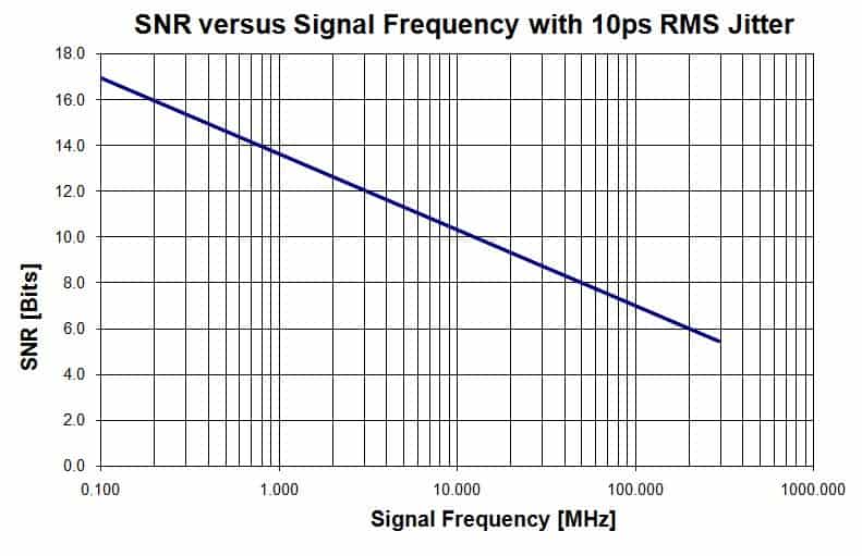
For data-converter clocking, the long-term jitter detracts from the SNR (signal-to-noise ratio) because SNR is 1/(2×π×F×σ), where F is the signal frequency, not the sampling frequency, and σ is the rms long-term jitter, which you can assume to be of a gaussian distribution. Figure 1 provides an example of the SNR versus frequency for an ADC using a clock with 10-psec-rms long-term jitter. High-speed, high-resolution ADCs require precise PLLs. Even 10 psec of rms long-term jitter limits the SNR of an ADC to 10 bits at slightly more than 12 MHz, 12 bits at 3 MHz, and 14 bits at slightly less than 1 MHz.
PLL operation
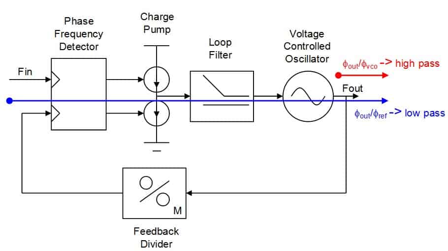
The operation of the charge-pump PLL involves many trade-offs among jitter, power, and area (Figure 2). Many ways exist for implementing PLLs, but most integrated PLLs use this topology. The feedback forces the output frequency, FOUT, to be equal to the input frequency, FIN, multiplied by the feedback-divide value, according to FOUT=FIN×M. Many PLLs also incorporate either an input or an output divider of value N to achieve a frequency FOUT=FIN×M/N.
A detailed frequency-domain analysis concludes that the PLL has both a highpass and a lowpass function (Reference 1). There is a lowpass function from input to output, meaning that reference phase noise below the PLL’s bandwidth passes through to the output, whereas noise higher than the loop’s bandwidth is attenuated. PLLs in noisy environments often use this feature to “clean up” a reference clock by attenuating high-frequency jitter.
The PLL has a highpass characteristic for VCO (voltage-controlled-oscillator) phase noise. Thus, the PLL attenuates VCO phase noise at low frequencies but passes noise above the loop bandwidth to the output. Ideally, all VCO noise would be attenuated through feedback, but PLLs, like all other feedback systems, face bandwidth limitations.
Sources of jitter
In a typical well-designed PLL, the largest phase noise or jitter source is the VCO. Many other noise sources exist, but you can usually make them smaller than that of a VCO with a modest area or power penalty. The charge pump and loop filter are usually the next-largest noise contributors. The loop filter can be either active or passive. In both cases, most PLLs usually use a zero resistor for loop stabilization. You can also make this noise insignificant by lowering the resistor’s value and increasing the integrating capacitor’s value and charge pump’s current to keep the loop gain constant. This approach has the undesired effect of increasing power and area.
The divider blocks usually contribute negligible device noise. However, a postdivider can be a significant source of short-term jitter due to power-supply noise. Supply noise can also contribute to long-term jitter through the charge pump, loop filter, and VCO, so be sure to design these blocks with sufficient supply-noise rejection.
Jitter and bandwidth
A frequency-domain analysis shows that jitter is suppressed below the loop bandwidth. The following time-domain experiments show that the PLL bandwidth is the link between short- and long-term jitter. You can perform two time-domain experiments using a signal analyzer or a scope to measure jitter (Figure 3 and Reference 2). The first experiment measures open-loop VCO jitter; the second measures the jitter of a PLL containing the VCO from the first experiment. Both experiments analyze the jitter by measuring the standard deviation of the zero crossings. They measure jitter versus time by using N hold-off times from 1×T to N×T, where T is the nominal period.
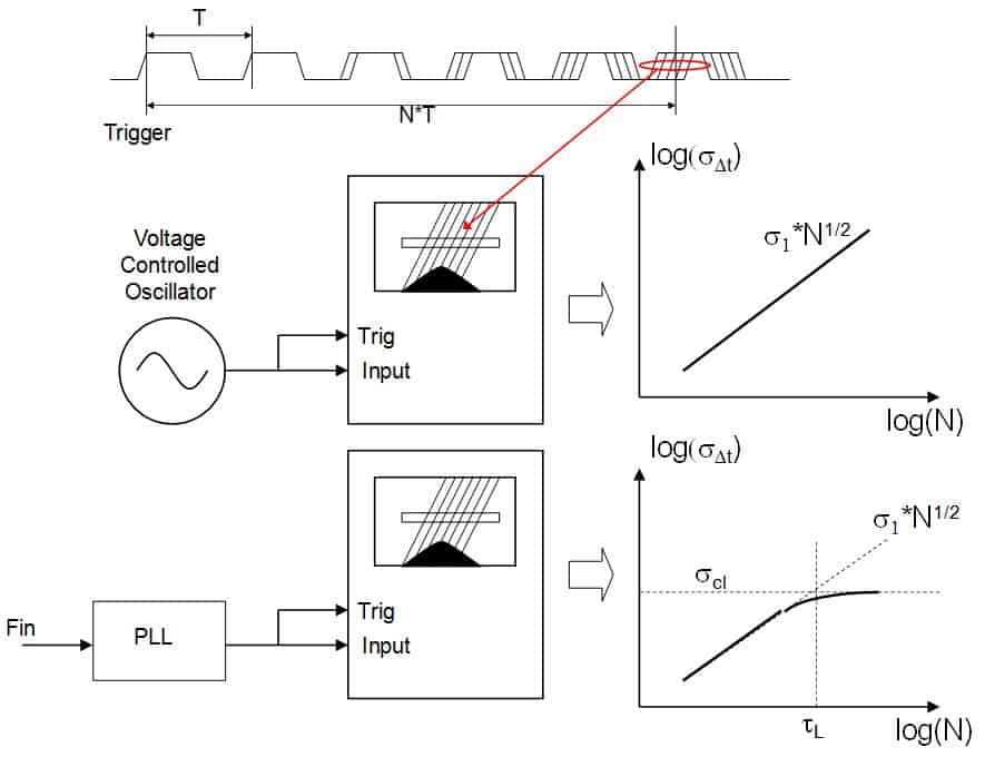
The first experiment measures the edges of an open-loop VCO. The standard deviation of the Nth zero crossing is the square root of N times the standard deviation of one cycle (σN=σ1×N1/2). The standard deviation of one cycle, σ1, is the period jitter. The value of σ1 is in practice difficult to measure due to the jitter of any buffer between the VCO and the measurement instrument. The short-term jitter of the instrument itself is also an error source. As N increases, the value of σNgrows without bound, whereas the rms jitter of the buffers has limits. Therefore, you can extrapolate the value of σ1from a plot of σN versus N.
A numerical example can highlight the difficulty in directly measuring σ1. Typical buffer noise for a broadband buffer is on the order of 30 fsec rms. The buffer noise adds in an rms way, so, for example, nine buffers with 30-fsec-rms noise in addition to the VCO with 110-fsec-rms jitter would cause no less than 200-fsec-rms cycle-to-cycle jitter. Additionally, supply noise can be as much as 100 fsec/mV on full-swing buffers, so it may be difficult to measure period jitter of less than 200 fsec in the time domain.
The second experiment measures the edges of a PLL with an ideal reference. The PLL contains the same VCO that the first experiment measured. For a few cycles, the measurements are almost identical to those of the open-loop VCO. You can expect this result because the PLL highpass-filters VCO noise. After many cycles, the measured standard deviation asymptotically approaches the closed-loop standard deviation or long-term jitter, σCL. The PLL is the force that bounds the phase error.
Figure 3 highlights a few important parameters. The closed-loop parameter σCL is a function of the PLL’s closed-loop bandwidth, τL, and the period jitter, σ1. The open-loop gain, which is a product of the charge-pump, loop-filter, and VCO gain divided by the feedback-divide value, determines the closed-loop bandwidth, a system-design parameter. You can calculate the closed-loop bandwidth, normalized to one VCO period, T, as 1/(2πFL/FVCO). You can now calculate the long-term jitter as σCL=σ1/(4πFL/FVCO)1/2 (Reference 2).
This analysis is a simplification in at least two ways. First, the only noise source it considers is VCO phase noise. However, VCO noise limits most well-designed PLLs. Note that this analysis does not consider supply noise or reference noise. The second simplification is that this analysis assumes the PLL to be a first-order loop. Most PLLs are at least second-order loops. Many PLLs are overdamped, however, and appear almost as first-order loops for the sake of this analysis. Additionally, the long-term jitter is a function of the square root of the bandwidth, so the error is not too severe for the sake of first-pass manual calculations.
These experiments yield two important results. The first result is that short-term period jitter depends almost entirely on the VCO and output buffers and does not depend on the PLL bandwidth. The second result is that long-term jitter depends on both the VCO’s and the PLL’s bandwidth, and it improves as the VCO improves and the bandwidth increases.
VCO phase noise
A pair of equal-power, 2-GHz oscillators consume several milliwatts (Figure 4). One oscillator is ring-based, and the other is LC-based. Three distinct regions of operation are shown in Figure 4. The most important is the −20-dB/decade region. This region typically determines the period jitter of the VCO, σ1.
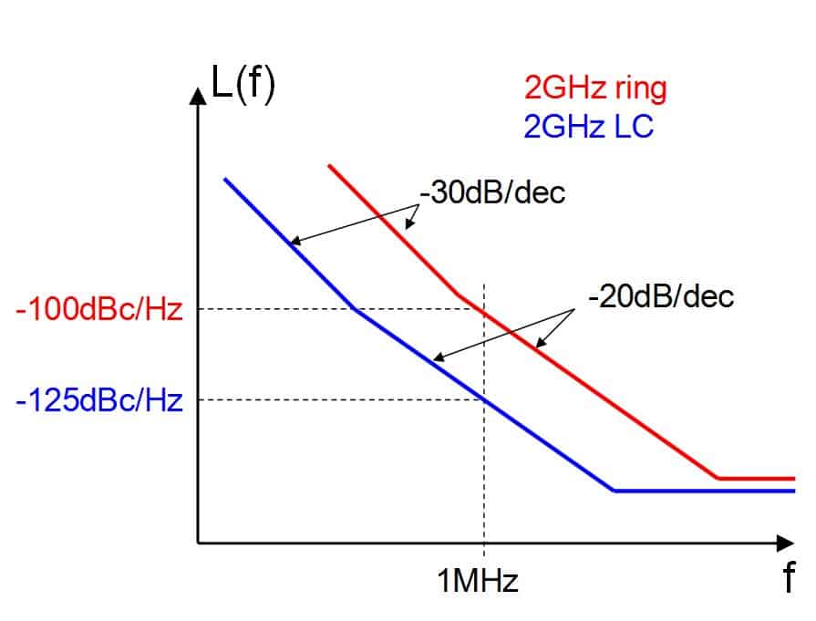
The plot also labels the −30-dB/decade region of the VCO. In this region, flicker device noise typically dominates over white noise, causing the increased slope. Because flicker noise is responsible for the increased slope, the transition from −30 dB/decade to −20 dB/decade is the flicker corner of the VCO. For ring-based VCOs, the flicker-noise corner typically ranges from 300 kHz to 3 MHz. For LC-based VCOs, you can obtain flicker-noise corners of less than 100 kHz. You should take care to optimize the VCO for flicker noise (Reference 3).
The plots also include a flat region at high frequencies, due to VCO output buffers. This region is important for period jitter but typically not important for long-term jitter, as the following equation shows: LdB(F)≈10×log10[(1/PSIG)×(FOSC)2/ (Q×F)2]. From this equation, the phase noise drops by 3 dB for a twofold increase in power for a given oscillator frequency. Increasing the power can be an effective way of improving the phase-noise performance but can become expensive. A 20-dB improvement in phase noise comes at a cost of a 100-fold power increase, with all other things constant. Another way of improving the phase noise is to increase the quality factor of the resonant tank. Doubling the quality factor halves the phase noise, a 6-dB improvement. The inductor structure often limits the achievable quality factor in a CMOS process. Typical quality factors range from seven to 15 and vary with many factors, including frequency and metal thickness. A trade-off also exists between tuning range and quality factor in LC VCOs in which a higher quality comes at the expense of a smaller tuning range.
There is roughly a 20-dB difference between the phase noise of a typical ring oscillator and that of an LC oscillator of the same power in a deep-submicron CMOS processes. This difference illustrates the phase-noise advantage of resonant-tank structures for phase noise.
As noted, the value of σ1 can be difficult to measure in the time domain. However, it is relatively straightforward in the frequency domain. You can calculate the VCO’s period jitter, σ1, as σ12=F2×L(F)/FOSC3, where F is the offset frequency, L(F) is the phase noise at F, and FOSC is the frequency of oscillation (Reference 4). In this example, the period jitter for the ring VCO with −100 dBc/Hz at 1-MHz offset and 2-GHz oscillation frequency is 112 fsec rms. The LC oscillator with −125 dBc/Hz at 1-MHz offset and 2-GHz oscillation frequency results in σ1 of 6.3 fsec rms. These values are typically too small to directly measure in the time domain, and buffer and scope noise obscure them.
You can calculate the long-term jitter from the PLL bandwidth and the corresponding value of σ1according to σCO=σ1/(4πFL/FVCO)1/2. Again, the calculations assume an overdamped PLL, VCO noise only, and no supply noise. Assuming a bandwidth of 100 kHz, the ring PLL with a σ1 of 112 fsec would have approximately 4.5 psec rms of long-term jitter, whereas the LC PLL with a σ1 of 6.3 fsec would have a long-term jitter of 270 fsec rms. If you increase the bandwidth to 1 MHz, then both long-term jitter values would decrease by to 1.4 and 85 fsec, respectively. You could continue these calculations for higher and higher bandwidths, but many reasons exist for limiting the bandwidth, and the jitter would not continue to decrease.
One of the primary factors limiting bandwidth is the PLL’s stability. Bandwidth is typically approximately only 1/20th of the reference rate for adequate phase margin. For high-performance PLLs, a low loop bandwidth mitigates reference-clock feedthrough. Suppressing reference-clock spurs typically requires a bandwidth of no more than 1/100th of the reference rate. Other reasons to limit the PLL bandwidth include delta-sigma modulation and reference-noise, loop-filter, and charge-pump noise suppression.
PLL area
Along with performance and power, area is a major specification for PLLs. The performance level of a PLL largely determines its area. You gain a large increase in performance by choosing an LC-based VCO rather than a ring-based VCO. The LC-based VCOs usually measure at least 300×300 microns for a design with one inductor and can be even larger. Ring oscillators, on the other hand, can measure 40×40 microns or smaller. Typically, LC oscillators have a narrower tuning range than do ring oscillators. Therefore, you must sometimes use multiple VCOs in the same PLL to achieve a wide tuning range, further increasing the area.
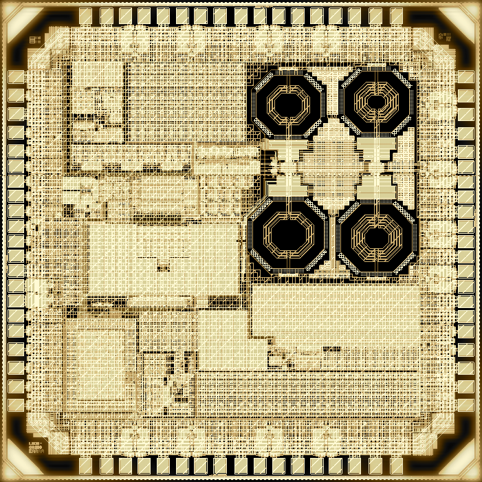
The loop filter is another part of the PLL that significantly increases in area with performance. An integrated loop filter can consume 500×500 microns or more. As the performance of the PLL drops, you can scale down the resistors, capacitors, and charge-pump current to reduce area at the cost of noise. You can make a SONET/multiprotocol clocking IC in 0.13-micron CMOS (Figure 5). The figure clearly shows the four-core LC VCO. The PLL measures roughly 1.4 mm2 in area. The long-term jitter is less than 500 fsec rms with a 50- kHz bandwidth. The PLL’s power dissipation is approximately 70 mW, depending on the mode of operation.
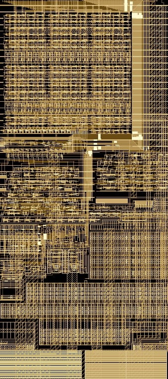
You can make a ring-based fractional-N PLL in 0.13-micron CMOS (Figure 6). The PLL’s area is 0.09 mm2, which is more than 10 times smaller than the LC PLL example in Figure 5. The long-term jitter is as low as 3 psec rms with a 1-MHz bandwidth, and the power consumption is approximately 5 mW, depending on the mode of operation. The area is largely digital. The digital blocks include a delta-sigma modulator, a predivider, a postdivider, feedback dividers, and control circuits. The analog area is more than 10 times smaller than that of the LC PLL analog area.
The two PLLs in figures 5 and 6 show why a one-size-fits-all approach does not work for SOC PLLs. The first PLL has jitter that is sufficient for almost all SOC applications. However, the area and power are both more than 10 times the area and power of the second example. The long-term jitter of the second example is six times higher, however, and would be almost 20 times higher if the PLLs had the same bandwidth.
The driving factor for many of the trade-offs of PLL SOCs is long-term jitter. If the long-term-jitter specification is loose, you can use a small, low-power, ring-based PLL. A tighter long-term-jitter specification entails the use of a lot of silicon area and power to meet the requirement with an LC-based PLL. However, for many applications between the two extremes, the choice is not clear, and you must perform careful analysis to optimize the PLL for power and area.
____________________________________________________________
This is a guest blog by Silicon Creations – provider of PLL and Mixed Signal Silicon IP Solutions