
Over the last several years, the buzzword in the electronics industry has been “More than Moore”, referring to the embedding of components into the package substrate and stacking of ICs and packages using wirebond and package on package (POP) technologies. This has led to the development of technologies that can lead to the ultra- miniaturization of electronic systems with coining of terms such as SIP (System in Package) and SOP (System on Package). More recently, the semiconductor industry has started focusing more on 3D integration using Through Silicon Vias (TSV). This is being quoted as a revolution in the electronics industry by several leading technologists. 3D technology, an alternative solution rdto the scaling problems being faced by the semiconductor industry provides a 3 dimension for connecting transistors, ICs and packages together with short interconnections, with the possibility for miniaturization, as never before. The semiconductor industry is investing heavily on TSVs as it provides opportunities for improved performance, bandwidth, lower power, reduced delay, lower cost and overall system miniaturization. Interposers play a very important role in such 3D integrated systems since they act as the conduit for supplying power, interfacing to the external world and handling the thermal management for 3D IC stacks.
Two different technologies are being proposed for the interposer today namely, silicon and glass. Though glass provides a low loss substrate solution it has its disadvantages which can be corrected using silicon. Similarly, silicon has several performance advantages but is limited due to the semiconductor properties of the substrate which can be corrected using glass. So, which provides a better alternative from an electrical
performance standpoint – silicon or glass?
In this paper, the electrical design and modeling challenges associated with 3D integration using TSVs is discussed with primary focus on the interposer. The results are contrasted with a glass interposer solution.
Through Silicon Via (TSV) is a new technology that provides short electrical connections between the top and bottom surface of a silicon substrate. When used in silicon stacking, TSVs provide short connections between transistors that are vertically separated from each other. The manner in which these connections are fabricated depend on whether via first, middle or last technology is used. In the area of packaging, TSVs used in silicon interposers also provide a short electrical path to the printed circuit board. What makes the modeling of TSVs interesting and its design challenging is the material properties of the medium surrounding these vertical interconnections. Due to the semi-conducting properties of the silicon medium; losses, capacitance effects and coupling behavior of TSVs are unique and are quite different for similar structures in a perfectly insulating medium. Hence, the electrical modeling of TSVs becomes important.
Silicon interposer technology is attractive since it enables the use of the existing semiconductor infrastructure for fabrication using earlier technology nodes. Since, the interposer does not contain any active devices and only contains passive interconnections, the interposers can be fabricated at a relatively lower cost. In addition, since the interposer has matched coefficient of thermal expansion (CTE) as compared to silicon, it acts as a buffer to relieve stresses between the chip stack and printed circuit board (PCB). However, due to the semiconducting properties of silicon, the vias and interconnections can create electrical design problems causing excessive coupling, which have been described in detail in this paper. Moreover, due to the multiscale dimensions of the interconnections used, extracting the parasitics of TSVs can be challenging depending on their density. To alleviate the electrical design problems associated with TSVs, alternate packaging solutions are being pursued such as the use of glass. The glass interposer solution is attractive since it provides very good insulating properties and can be fabricated in large panels, thereby potentially reducing the cost even further as compared to the silicon interposer. However, glass has a higher CTE as compared to silicon and has a thermal conductivity lower than silicon, causing hot spots, more so than silicon.
In this paper, the electrical design and modeling of TSVs used in interposers and in ICs (to a lesser extent) are discussed in detail followed by some results on the glass interposer. The two are then compared from a signal and power integrity standpoint, especially for high speed I/O signaling.
2.A. Benefits of Through Silicon Vias
As is well known, TSVs provide short interconnection lengths as opposed to wirebond technology for stacking of ICs. Recent studies have shown that 3D DDR3 DRAM [Kang et al, 2010] can be enabled by using TSVs whereby 50% reduction in standby power and 25% reduction in active power is possible as compared to quad-die package with an increase in I/O speed from 1066Mbps to 1600Mbps. An emerging application is in the area of wide I/O memory for mobile applications where logic and memory are being stacked on top of each other using TSV technology. In an interesting plenary talk given by Oh Hyun Kwon [ISSCC, 2010], he compared a conventional 3D package using Flip Chip Package on Package with LPDDR2 memory (low power DDR2) to an equivalent System in Package (SiP) with wide IO memory, as shown in Figure 1. Dramatic improvements in package size (35% reduction) and power consumption (50% reduction) were seen as shown in Figure 1(c). A very interesting aspect is the increase in bandwidth by 8X by supporting 512 I/Os transmitting at a data rate of 12.8Gbps as compared to 3.2Gbps in LPDDR2 memory.
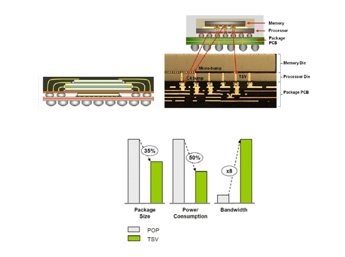
Figure 1: (a) FC-POP, (b) TSV-SiP with wide I/O DRAM an d (c) Performance Benefits
The reduction in package size is obvious since the wirebonds on the top tier in the memory stack in Figure 1(a) is around 1mm long, thereby using a large amount of area to package the memory stack as opposed to the flip chip processor in the bottom package. By replacing the wirebonds using TSVs in Figure 1(b), the interconnection length and therefore the package area can be reduced. The reduction in power can be attributed to the reduction in the capacitance of the TSV-SiP that needs to be charged and discharged as compared to the wirebond and routing capacitance in the FC-POP. Finally, the higher bandwidth for SiP-TSV is due to the fine pitch of the TSVs that provide more interconnections per unit area as compared to FC-POP, leading to 512 signal I/O connections (total connections is around 1200 including power and ground) between the processor and memory. Due to the shorter delay of TSVs due to the smaller interconnection length (1mm long wirebond as compared to 60m long TSV), the speed of the processor-memory interface has increased from 3.2Gbps to 12.8Gbps. Clearly, the parasitics of the interconnections dictate to a large extent the electrical performance of either the FC-POP or TSV-SiP.
2.B. Integration Approaches
Currently three integration approaches are being pursued for system integration namely 1) 3D integration using chip stacking where the chips are interconnected to each other using TSVs and mounted on a silicon interposer or directly on a PCB, as shown in Figure 2 (a). The second approach is a 3D enabled approach where the silicon or glass interposer is used to connect chips to each other using TSVs or Through Glass Vias (TGV) as shown in Figure 2 (b). The third approach being touted as a 2.5D approach uses a silicon interposer with fine lines and vias to connect chips to each other, similar to a Multi-Chip Module which is then mounted on a PCB, as illustrated in Figure 2 (c). The solution in Figure 1(a) is currently being pursued by the mobile industry led by Samsung while Xilinx is pursuing the solution shown in Figure 2 (c) to reduce chip size (improves yield) and enable high throughput for FPGA based applications. The solution in Figure 2 (b) is currently at a research phase, with a lot of interest from system companies since it provides the ability to connect chips together without having to create TSVs in the logic chip, thereby providing more room for transistors and reducing stresses in the IC. The challenges in the electrical design aspects of the problem are similar for these integration approaches with some differences. Hence, the material presented in this paper should cover all these integration approaches.
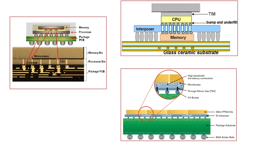
Figure 2: System Integration approaches (a) Chip stacking using TSVs on
PCB (courtesy Samsung), (b) Interposer enabled 3D solution and (c) 2.5D
solution using TSVs (courtesy Xilinx)
3.A. Challenges
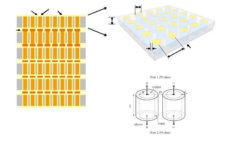
Consider a silicon stack as shown in Figure 3 (a) containing multiple tier, where each tier represents a die. The tiers are bonded to each other through microbumps or pads. Without loss of generality, the bottom most tier could be considered as the silicon interposer. The physical geometry associated with one of the tiers is enlarged in Figure 3 (b) showing the copper connections at the center of the TSV, surrounded by an oxide liner in a silicon medium. Depending on the process used, copper can be substituted with tungsten which provides a better Coefficient of Thermal Expansion (CTE) match to the silicon substrate but at the expense of higher resistance. The structure shown in Figure 3 (b) is also used in silicon interposers to package the stacked ICs. Two of the TSVs are shown in Figure 3 (c) to illustrate the physical geometry and material properties.
Read the complete article here.
_______________________________________________________________________
This is guest post by Madhavan Swaminathan Founder of E-System Design, an EDA company focusing on CAD solutions for integrated microsystems, where he serves as the Chief Technical Officer.