

While assembly houses are gradually becoming more and more organized in regards to following internal processes, it seems that we, their customers, are often trying to push them to make shortcuts only because “we are running out of time”.
With chip design cycle time shrinking, production related tasks such as packaging and test are de-prioritized. Yet, designing a package takes time, and without a proper package performance is impacted.
The first step is submitting your package design files to the assembly engineering team. We put together a checklist of the key items you should be prepared to deliver. For demonstration purposes we created a list of deliverables for a QFN package type. The details may vary between different packaging houses, but the general guidelines and expectations are the same.
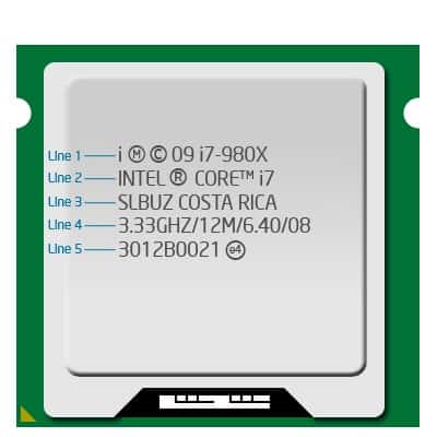
In this document you specify the package topside marking which provides important information about the device. In addition to helping you or your customers identify the device, the marking details should provide information on manufacturing date.
For the packaging marking specification, you’ll need to deliver one document and one image file. The amount of data that can be placed on the package will depend on the package size, but will typically include:
Company Logo – black-white logo, with the right orientation relative to pin #1
Company name – your company name
Chip Part number – your chip name
Lot trace code – use the number of you wafer lot
Date code – week number and year
Pin #1 identifier – mark the location of pin #1
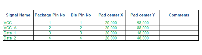
The Netlist document defines the connections between the die pads and the package pins. It should be a table that consist of 5 columns: Signal Name, Die Pad number, Package pin number, pad location (X, Y), and comments.
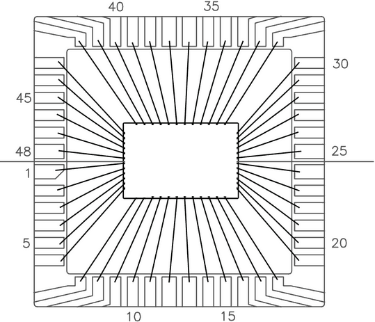
The Bond diagram shows a top view drawing of the die, the pads, the package pins and all the wirebonds to be wired by the assembly house.
Creating the diagram in the right perspective will help you realistically visualize your final product. For example, where do you have long wirebonds, short wirebonds, etc. The diagram should also show all the required downbonds. For clarification, write down the (die) pad number and the (package) pin number, next to every pad and pin. Make sure the numbering is aligned with your design files. This document can be delivered in PDF format.
You are welcome to add additional ideas for our packaging checklist, or browse our listed IC packaging providers.
As you may have guessed, this document provides a general information about the project, such as: customer name and contact information, project name, wafer size, wafer thickness, wafer map, package details, pad opening and die size.
It’s highly recommended to review all the documents internally before sending them out — only to ensure there are no mistakes and all the information is correct and nothing is missing. A second pair of eyes that reviews all data is always recommended. When the files are ready, you can add a revision number (for tracking purposes), zip all files to a single compressed file and email it to the assembly house.
While this all sounds quite trivial, delivering complete information will help you avoid multiple, time-consuming iterations between you and the packaging house, which can take days and even weeks due to different time zones.
You can learn more about packaging vendors in our IC Packaging section.


