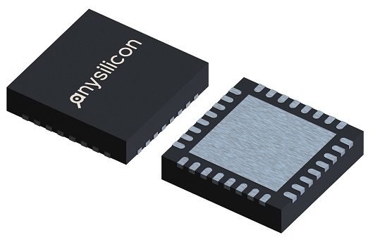
Looking for a QFN packaging company for prototype, low-volume or production assembly?
AnySilicon helps semiconductor companies connect with IC packaging and assembly providers offering standard and custom QFN packaging services worldwide.
Submit your die, package and volume requirements and AnySilicon can help identify suitable packaging partners for QFN, DFN, PQFN, multi-row QFN, flip-chip QFN and other leadframe-based package requirements.
Need a QFN packaging quote?
Send us your package type, die size, number of pins, wafer size, expected volume and project status. We can distribute your requirement to relevant IC packaging companies.
Get QFN Packaging Quotes →
Find QFN Packaging and Assembly Services
QFN packaging is a widely used semiconductor assembly option because it combines a compact footprint with good electrical and thermal performance. The package is generally built around a copper leadframe, with the silicon die attached to the center paddle and connected to the leads using wire bonding or, in some configurations, flip-chip interconnect.
Depending on your project, a QFN packaging supplier may provide:
- Package selection and feasibility review
- Open-tool QFN package selection
- Custom QFN leadframe design
- Wafer backgrinding
- Wafer dicing
- Die attach
- Gold, copper or other wire-bonding options
- Flip-chip assembly where applicable
- Transfer molding
- Package singulation
- Laser marking
- Electrical final test
- Reliability qualification
- Tape-and-reel or other final packing
AnySilicon’s packaging RFQ service allows semiconductor companies to submit a project once and have the requirement distributed to relevant assembly and packaging companies.
QFN Package Types Supported by Packaging Companies
QFN is a package family rather than one fixed package. The appropriate structure depends on die size, I/O count, thermal requirements, electrical performance, application and production volume.
| QFN Type |
Typical Use |
Key Considerations |
| Standard QFN |
General analog, digital, mixed-signal and power ICs |
Body size, pin count, pitch, exposed pad and open-tool availability |
| DFN |
Low-pin-count and compact devices |
Two-sided lead arrangement and small footprint |
| PQFN / Power QFN |
Power-management and power-semiconductor applications |
Thermal path, exposed pads, current capability and die attach |
| Multi-Row QFN |
Higher-I/O devices requiring a compact leadframe package |
Multiple lead rows, routing, leadframe availability and assembly process |
| Flip-Chip QFN |
RF, high-speed or performance-sensitive applications |
Die bumping, interconnect structure, assembly complexity and cost |
| Multi-Die QFN / SiP |
Multiple dies or functions inside one molded package |
Die placement, wire-bond clearance, thermal behavior and test strategy |
| Custom QFN |
Projects not fitting an existing open-tool package |
Leadframe tooling, NRE, qualification, minimum order and schedule |
For a broader technical overview of package structure, exposed pads, leadframes, lead counts and package variants, see the AnySilicon QFN Package Guide.
Typical QFN Assembly Process
The exact process flow varies by assembly house and package configuration, but a typical QFN project can include the following stages:
- Package definition: select an open-tool package or create a custom leadframe.
- Wafer preparation: backgrind if required, followed by wafer dicing.
- Die attach: attach known-good die to the QFN leadframe paddle.
- Interconnect: wire bond die pads to leadframe fingers or use a suitable flip-chip approach.
- Molding: encapsulate the die and interconnect structure.
- Singulation: separate individual packages by sawing or another supported process.
- Marking and inspection: apply package marking and perform visual or other inspections.
- Final test: electrically test packaged devices if required.
- Packing and shipment: tray, tube or tape-and-reel depending on product requirements.
What Information Is Needed for a QFN Packaging Quote?
A detailed request helps packaging suppliers determine whether an existing QFN platform can be used and reduces the time needed to prepare a meaningful quote.
| Information |
Example |
Why It Matters |
| Package type |
QFN, DFN, PQFN, multi-row QFN |
Defines the basic package platform |
| Die size |
3.2 mm × 3.8 mm |
Determines fit, paddle size and wire-bond geometry |
| Die thickness |
150 µm |
Affects package height and die handling |
| Number of I/Os |
48 pins |
Used to identify suitable leadframes and body sizes |
| Preferred body size |
7 mm × 7 mm |
Helps determine whether an open tool is available |
| Wafer size |
200 mm |
Determines wafer handling and dicing requirements |
| Input form |
Wafer, sawn wafer or singulated die |
Defines which upstream assembly steps are needed |
| Wire-bond requirement |
Copper or gold wire |
Affects process compatibility and cost |
| Annual volume |
250,000 units/year |
Important for unit pricing, tooling and capacity planning |
| Prototype quantity |
500 units |
Helps determine engineering-lot feasibility |
| Qualification |
Industrial or automotive |
Changes material, process and reliability requirements |
| Test requirement |
Assembly only or assembly + final test |
Determines overall service scope |
Already know your package requirements?
Submit your project and let AnySilicon distribute it to suitable IC packaging companies.
Request QFN Packaging Quotes →
What Determines QFN Packaging Cost?
There is no single universal QFN package price. The final assembly cost depends on package configuration, tooling, materials, processing requirements and production volume.
Important cost drivers include:
- Open-tool package versus custom leadframe
- Package body size
- Pin count and pitch
- Die size and thickness
- Number and length of wire bonds
- Gold versus copper or other interconnect options
- Exposed-pad and thermal requirements
- Wafer backgrind and dicing
- Mold compound and reliability requirements
- Prototype versus volume-production quantity
- Final test and qualification scope
- Assembly region and logistics
An existing open-tool package can often reduce NRE and schedule compared with creating a completely custom leadframe. However, die dimensions, pad arrangement, I/O count and thermal requirements still need to be compatible with the selected package.
For an early cost indication, use the AnySilicon IC Package Price Estimator. The estimator supports semiconductor package cost planning and can also be used to request price quotes from assembly vendors.
Prototype and Low-Volume QFN Packaging Services
Startups, universities, defense programs, sensor companies and fabless semiconductor companies frequently need QFN assembly before their production volume is large enough for a conventional high-volume OSAT engagement.
Low-volume projects may involve:
- Engineering samples
- Prototype ASICs
- MPW shuttle dies
- Qualification lots
- Pilot production
- Low-volume industrial products
- Specialty or long-lifecycle semiconductor products
The main challenge is finding a packaging company willing to support the required volume while also having a compatible QFN platform.
When possible, provide both your initial prototype quantity and expected annual production volume. This gives suppliers a clearer picture of the project’s potential lifecycle.
QFN Packaging for Volume Production
Production QFN programs typically require more than a package unit price. The assembly partner must also meet capacity, quality, traceability, reliability and supply-chain requirements.
For production programs, consider:
- Monthly and annual capacity
- Yield targets
- Lot traceability
- Change-control and PCN procedures
- Material control
- Reliability qualification
- Automotive or industrial quality requirements
- Final test and outgoing quality controls
- Business-continuity and second-source considerations
Open-Tool QFN vs. Custom QFN Leadframe
One of the first commercial decisions is whether the project can use an assembly house’s existing QFN tooling or requires a custom leadframe.
| Option |
Advantages |
Considerations |
| Open-Tool QFN |
Potentially lower NRE and faster start |
Die size, pin count, exposed pad and bond geometry must fit available tooling |
| Custom QFN Leadframe |
Greater freedom to optimize pinout, exposed pad, body size and die fit |
Additional tooling/NRE, development time and qualification may be required |
How to Select a QFN Packaging Company
The lowest unit price is not always the best supplier-selection criterion. A packaging company should also match the technical, volume and quality needs of the program.
Questions to ask include:
- Do you have an existing QFN tool compatible with our die and pin count?
- What is the minimum practical engineering-lot quantity?
- Can you support our expected production volume?
- Which wire-bond materials and die-attach options are available?
- Can you perform wafer backgrind and dicing?
- Can you support package design and bonding-diagram review?
- Which reliability and qualification services are available?
- Can you provide final test?
- What are the NRE, tooling and lead times?
- What quality systems and traceability processes are used?
You can also browse the AnySilicon IC Packaging Vendor Directory to review semiconductor packaging companies and their capabilities.
Find a QFN Packaging Company
Provide as much information as possible:
- QFN type and preferred body size
- Die dimensions and wafer size
- Pin count and bonding requirements
- Prototype and annual volumes
- Qualification and test requirements
- Required schedule
Get 3 Quotes from IC Packaging Companies →
Frequently Asked Questions
Where can I find QFN packaging services?
QFN packaging is offered by semiconductor assembly houses, OSAT providers and specialty IC packaging companies. AnySilicon can distribute a QFN project requirement to relevant packaging suppliers through its IC packaging RFQ service.
What information do I need for a QFN packaging quote?
Suppliers typically need the die dimensions, wafer size or die input format, pin count, preferred package dimensions, annual volume, initial build quantity and any reliability, thermal, test or qualification requirements.
Can I get QFN packaging for low volumes?
Yes. Some specialty packaging companies support prototypes, engineering lots and low-volume production. Availability depends on package tooling, die dimensions, materials and the minimum lot size supported by the assembly provider.
How much does QFN packaging cost?
QFN packaging cost depends on package size, pin count, leadframe tooling, die size, wire-bond configuration, production volume, wafer-preparation requirements, qualification and test. An open-tool package can often reduce NRE compared with a fully custom leadframe.
What is an open-tool QFN package?
An open-tool QFN is an existing package platform already available at an assembly house. If the die dimensions, pin count, exposed pad and bonding geometry are compatible, it may reduce tooling cost and shorten the package-development schedule.
Can QFN packages use copper wire bonding?
Yes. Copper wire bonding is widely used in semiconductor packaging, but compatibility depends on the die pad structure, assembly process and reliability requirements. The assembly provider should review the specific die and process requirements.
What is the difference between QFN and BGA packaging?
QFN is generally a leadframe-based package with peripheral or multi-row contacts, while BGA uses an array of solder balls and typically a package substrate. BGA is often selected when a design requires more I/Os or different routing capability, while QFN can be attractive for compact, cost-sensitive designs when the required I/O count and performance fit the package.