



QFN is usually the better choice when your priorities are minimum PCB area, short electrical paths, RF/high-frequency performance and efficient heat transfer into the PCB; QFP is usually the better choice when visible solder joints, easier optical inspection, probing and rework are more important. The fundamental difference is mechanical: a QFN (Quad Flat No-Lead) package uses bottom/perimeter lands with no protruding leads and often a large exposed center pad, while a QFP (Quad Flat Package) uses visible gull-wing leads extending from all four sides. That makes QFN compact and electrically efficient, but its hidden, low-standoff solder joints demand tighter PCB/assembly control. QFP occupies more board area and has longer electrical paths, but its compliant external leads make manufacturing inspection and repair considerably easier.
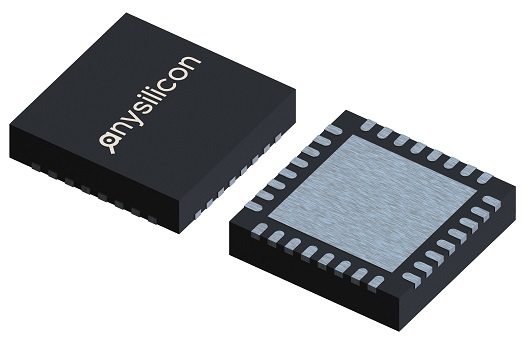
Figure 1: QFN Package
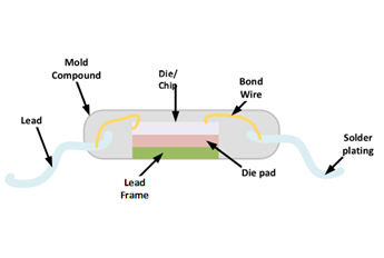
Figure 2: QFP Package
For an ASIC, MCU, analog, RF or mixed-signal device, package selection should not be based on size alone. The package affects electrical parasitics, thermal resistance, solder-joint fatigue, board layout, inspection strategy, production yield, rework cost and long-term reliability.
| Feature | QFN | QFP |
|---|---|---|
| Full name | Quad Flat No-Lead | Quad Flat Package |
| PCB connection | Bottom/perimeter lands; no protruding leads | Visible gull-wing leads on four sides |
| PCB footprint | Smaller | Larger because leads extend outside the body |
| Package height | Typically low profile | Generally higher than comparable QFN variants |
| Electrical path | Short | Longer due to external leads |
| RF / high-frequency suitability | Generally stronger | Good for many applications, but lead parasitics are higher |
| Thermal path | Often excellent through exposed center pad into PCB | Depends on package style; usually less direct than exposed-pad QFN |
| Solder-joint visibility | Mostly hidden underneath package | Visible around package perimeter |
| AOI inspection | Limited unless side-wettable features are provided | Generally straightforward |
| Rework | More difficult | Generally easier |
| Thermal-cycle compliance | Low standoff; demands careful design | Gull-wing leads provide greater mechanical compliance |
| Typical reason to choose | Compact size, RF, thermals, low parasitics | Inspectability, accessibility, reworkability |
QFN stands for Quad Flat No-Lead. It belongs to the broader family of bottom-termination components (BTCs). Instead of using leads that extend outside the package, the electrical terminals are integrated into the underside/perimeter of the package body.
Most conventional QFNs are plastic-molded packages built around a copper lead frame. The die is attached to a central paddle, wire bonded or otherwise connected to the perimeter terminals, and encapsulated. On the underside, the package normally exposes the perimeter connection lands and a large center pad.
The center pad can serve several functions:
The NASA/JPL review of QFN technology identifies lower cost, reduced package size and improved functionality – especially for RF applications – as major drivers for QFN adoption. It also emphasizes that the absence of conventional leads changes the assembly and reliability behavior of the package.
QFP stands for Quad Flat Package. It is a mature surface-mount package in which leads extend from all four sides of a square or rectangular molded body.
The leads normally bend downward and outward in the characteristic gull-wing shape. This creates a visible solder joint between each lead and its PCB land.
AnySilicon’s QFP guide describes QFP as a widely used package for microprocessors, memory, embedded control, communication and industrial applications. Typical QFP families span a broad range of I/O counts, and the guide notes examples from roughly 32 to 304 pins with lead pitches commonly in the 0.4 to 1.0 mm range.
The external leads are the defining difference from QFN. They consume more board area, but they also provide mechanical compliance and make the solder joints accessible to optical inspection, probing and repair.
The QFN-versus-QFP decision is fundamentally a choice between leadless bottom termination and external compliant leads.
| Package Element | QFN | QFP |
|---|---|---|
| External leads | No protruding leads | Gull-wing leads extend outside package |
| Solder location | Primarily underneath package | Along visible perimeter |
| Center exposed pad | Common | Available on some enhanced variants, but not the defining architecture |
| Board-to-package standoff | Low | Greater because of formed leads |
| Mechanical compliance | Lower | Higher because the leads can flex |
NASA’s QFN reliability review points out that leadless packages do not have leads or solder balls to absorb distortion from package and PCB warpage. This is why QFN board design, solder-paste deposition and assembly control become particularly important.
QFN generally has the advantage when PCB area is constrained.
Because the QFN terminals are located underneath and near the package edge, the PCB footprint stays close to the molded package dimensions. A QFP requires additional board area around the body for the gull-wing leads and their solder lands.
This makes QFN particularly attractive for:
QFP remains compact compared with older through-hole packages and can accommodate substantial pin counts, but it normally requires a larger PCB keep-out area for the same body size.
QFN generally has the electrical advantage.
Every package interconnect introduces parasitic resistance, inductance and capacitance. Long package leads increase the electrical distance between silicon and PCB. QFP’s gull-wing leads are practical and manufacturable, but the lead length contributes additional parasitic inductance and capacitance.
QFN shortens this path considerably. The connection moves directly from the lead frame to a bottom land and then into the PCB.
The NASA/JPL report specifically highlights the electrical and RF advantages of leadless packaging. In one cited QFN implementation, the exposed die-attach pad provided both heat conduction and a stable ground path. The report also describes advanced QFN testing that demonstrated strong high-frequency performance compared with a fine-pitch BGA reference design.
QFP remains suitable for a wide range of microcontrollers, digital logic, industrial control, embedded processing and moderate-speed interfaces. Its electrical penalty only becomes decisive when package parasitics are significant relative to the electrical requirements of the device.
Thermal design is one of QFN’s strongest advantages when the package includes an exposed center pad.
The QFN die-attach paddle can be soldered directly to a corresponding thermal pad on the PCB. Heat then flows from the silicon through the exposed pad and into copper planes in the board.
NASA’s assembly guidance emphasizes that the exposed pad should be soldered to the PCB for enhanced thermal, electrical and board-level performance. Thermal vias can then connect the top-side thermal land to internal or backside copper planes.
Current Infineon QFN assembly guidance follows the same principle: the exposed pad is not only an electrical connection, but a key thermal path into the PCB. The optimum via pattern depends on device power, board construction and application requirements.
A QFN only delivers its thermal potential when the PCB land pattern and solder process are designed correctly. Too little solder can reduce thermal contact. Too much paste beneath the center pad can lift the package and reduce the quality of the perimeter joints.
NASA’s review identifies solder-paste volume as one of the central QFN assembly-control issues. The report also recommends segmented stencil openings rather than one large aperture for the center pad, helping manage outgassing, void formation and package float during reflow.
QFP can also be engineered for effective heat dissipation, including thermally enhanced versions, but a standard gull-wing QFP does not inherently provide the same large bottom-side thermal path as an exposed-pad QFN.
A common simplification is that “QFP is high pin count and QFN is low pin count.” That is no longer universally true.
Conventional perimeter QFN packages are indeed often used at moderate I/O counts. However, NASA’s review documents dual-row, multi-row and advanced QFN structures specifically developed to increase I/O density.
The report notes that advanced QFN I/O counts can approach chip-scale package and fine-pitch BGA territory. It discusses tested examples including a 164-I/O dual-row QFN and a 236-I/O three-row QFN.
| I/O Consideration | QFN | QFP |
|---|---|---|
| Conventional package | Usually low to moderate I/O | Strong range of moderate to high I/O |
| Advanced versions | Dual-row / multi-row QFN significantly extends I/O count | Fine-pitch QFP variants extend pin density |
| PCB escape routing | Compact, but internal rows can increase routing complexity | Leads fan outward and are easy to access, but consume perimeter space |
| Very high I/O | Possible with advanced QFN, but BGA may become more attractive | Possible within QFP limits, but package size and fine pitch become challenging |
Both packages are standard surface-mount devices, but the assembly process window differs significantly.
QFN has no pre-attached solder balls and no external lead shape to create the joint geometry. Solder paste printed onto the PCB provides the solder for both perimeter terminals and the exposed pad.
NASA’s QFN review identifies two recurring process issues:
The center pad makes stencil design particularly important. If a large amount of solder is deposited under the exposed pad, the molten solder can raise the package during reflow and reduce the solder available for effective perimeter fillets or change the final stand-off.
For that reason, QFN exposed-pad stencil patterns commonly use an array of smaller apertures rather than one large opening.
QFP assembly is mature and well understood. Solder paste is printed on the PCB pads, the component is placed, and the gull-wing leads form visible solder fillets during reflow.
The main manufacturing concerns are different from QFN:
The external leads generally make process results easier to observe and troubleshoot.
QFP clearly wins on inspection simplicity.
With QFP, the gull-wing leads and solder joints are exposed around the body. Automated optical inspection (AOI) can assess alignment, solder fillets, bridging and many other defects without looking underneath the package.
QFN is fundamentally different because the majority of the solder joint exists underneath the body.
The NASA/JPL report states that visual inspection can examine the outer termination area, but it cannot determine the integrity of the hidden portion of the solder joint. The large center-pad connection is also hidden. X-ray is therefore important for identifying voids, solder bridging, missing solder and other concealed features.
Current Infineon QFN guidance makes the same distinction: conventional AOI may not reliably characterize standard QFN joints because they are primarily underneath the package. Packages with intentionally wettable side features can improve optical inspection capability.
| Inspection Method | QFN | QFP |
|---|---|---|
| Visual inspection | Limited | Very useful |
| AOI | Limited for hidden joints; improved by wettable flank designs | Well suited |
| X-ray | Frequently useful for hidden joints and exposed-pad voids | Usually less essential for basic perimeter-joint inspection |
| Cross-section | Useful for detailed process/reliability investigation | Usually reserved for failure analysis |
QFP is generally easier to rework because the technician can see and access the leads.
Current Infineon guidance for gull-wing packages explicitly treats them as reworkable using appropriate rework equipment, while also warning that very fine-pitch individual-joint repair can be difficult.
QFN rework normally requires heating and removing the entire package because individual bottom joints cannot be accessed directly. The center thermal pad also increases the thermal mass involved in removal and replacement.
This can matter during:
If you expect substantial manual debug or rework during early development, QFP can offer a practical advantage even when QFN would produce a smaller final product.
This is one of the most important tradeoffs – and one of the reasons package selection should consider the application’s environment.
NASA’s QFN review stresses that the low stand-off and absence of compliant external leads can make QFN solder joints more sensitive to differential expansion between the package and PCB during thermal cycling.
QFP’s gull-wing leads provide a longer, more flexible mechanical path. That compliance can absorb some relative movement between component and board.
The reviewed reliability studies showed that QFN fatigue life is strongly influenced by package geometry and assembly details. Important factors included:
One cited study showed that increasing board thickness reduced QFN solder-joint reliability under the tested thermal-cycling conditions. Other work showed substantial improvement when QFN stand-off and joint geometry were increased.
Because the exposed QFN center pad creates a large solder area, void formation during reflow is a recurring manufacturing concern.
NASA’s review notes that voids can affect thermal and high-frequency behavior because they reduce effective metal contact and may lengthen current paths. It also reports package-specific thermal simulation in which multiple smaller distributed voids covering up to roughly half of the pad area did not significantly change thermal performance, while large localized voids remained undesirable.
This should not be interpreted as a universal acceptance limit. The acceptable void level depends on:
For production, the component vendor’s recommended land pattern and stencil design should take priority over generic rules.
For demanding environments, there is no automatic winner.
QFN can be highly attractive because it is compact, thermally efficient and electrically strong. But thermal-cycle reliability, hidden-joint inspection and PCB warpage need careful attention.
QFP gives up some size and electrical efficiency in exchange for visible joints and compliant leads. In systems where inspection and repair are critical, that can be a major advantage.
For automotive use, QFN variants with wettable flanks or side-wettable features are increasingly useful because they provide a solder fillet that can be inspected optically. They address one of standard QFN’s biggest production-quality challenges without giving up the basic leadless architecture.
Package cost should be evaluated at the system level rather than only by the package purchase price.
NASA’s QFN review notes that lead-frame QFN can be cost-effective because it avoids the substrate required by packages such as BGA. A conventional QFN itself can therefore be an economical packaging solution.
However, manufacturing cost can move in the opposite direction if the application requires:
QFP is also a mature, cost-effective package family. Its larger PCB footprint may add system cost, while easier inspection and rework can reduce manufacturing and debug expense.
| Cost Area | QFN | QFP |
|---|---|---|
| Package material / structure | Generally economical lead-frame architecture | Mature and economical lead-frame architecture |
| PCB area | Lower | Higher |
| Inspection | May require X-ray or enhanced process control | AOI / visual inspection is easier |
| Rework | More difficult | Generally easier |
| Thermal solution | PCB thermal vias often required for high-power devices | Application dependent |
QFN is usually the stronger candidate when:
QFP is usually the stronger candidate when:
| Application | Likely Preference | Why |
|---|---|---|
| RF transceiver / front end | QFN | Short electrical paths, low parasitics and exposed ground pad |
| Power-management IC | QFN | Compact size and strong heat path into PCB |
| Compact consumer device | QFN | Low profile and small PCB footprint |
| Prototype MCU board | QFP | Visible pins are easier to probe, inspect and rework |
| Industrial controller | Depends | QFP favors accessibility; QFN favors compactness and thermals |
| High-reliability wide-temperature system | Application-specific | Requires package-specific thermal-cycle and board-level validation |
| High-volume compact ASIC | Often QFN | Efficient footprint and cost once assembly process is controlled |
| Low-volume board requiring frequent repair | Often QFP | Accessible solder joints simplify rework |
Package selection is only one part of the decision. The same QFN can perform very differently on two PCBs because of differences in pad geometry, thermal vias, board thickness, copper distribution and solder-paste printing.
Before finalizing QFN or QFP, define:
For QFN in particular, use the package supplier’s recommended land pattern and stencil design rather than treating all QFNs as geometrically interchangeable.
| If Your Priority Is… | Better Starting Point |
|---|---|
| Smallest PCB footprint | QFN |
| Lowest package parasitics | QFN |
| RF / high-frequency performance | QFN |
| Direct heat transfer to PCB | QFN |
| Easy optical inspection | QFP |
| Easy access for probing | QFP |
| Easy rework | QFP |
| Mechanical lead compliance | QFP |
| High I/O in compact leadless format | Advanced / multi-row QFN may fit |
| High reliability over severe thermal cycling | Evaluate the exact package, PCB and qualification data |
QFN has no external leads. Its electrical terminals are mainly located underneath and around the perimeter of the package, often together with a large exposed center pad. QFP uses visible gull-wing leads extending from all four sides.
Not universally. QFN is normally better for compact size, thermal transfer and low-parasitic electrical performance. QFP is normally better for visual inspection, pin accessibility and rework.
QFN is generally preferred for RF and high-frequency applications because the shorter electrical paths reduce package parasitics and the exposed pad can provide a low-inductance ground connection.
Both are routinely assembled with standard SMT processes, but QFP gives more visible process feedback. QFN requires tighter control of stencil design and solder volume, particularly underneath the exposed center pad.
Yes. Advanced dual-row and multi-row QFN packages have extended QFN well beyond traditional low-to-moderate I/O counts. NASA’s review includes examples at 164 and 236 I/O.
Most of the solder joint is hidden underneath the package. Visual inspection can only see the package edge, while X-ray may be needed to evaluate concealed joints and center-pad voiding. Wettable-flank QFN variants can improve optical inspection.
QFP is generally easier because the leads are visible and accessible. QFN normally requires removal and replacement of the entire package.
AnySilicon can connect semiconductor companies with packaging and assembly suppliers for QFN, QFP, BGA, WLCSP, flip-chip and other IC package types.
Related AnySilicon resources: Ultimate Guide to QFN Package, Ultimate Guide to QFP Package, and QFN Packaging Services.
