Developing a custom sensor interface ASIC requires specialized expertise in analog design, signal conditioning, data conversion, low-noise circuits and semiconductor manufacturing.
Whether your application involves industrial sensors, medical devices, MEMS, automotive systems or precision measurement equipment, a custom sensor ASIC can help reduce system size, lower power consumption, improve signal quality and integrate multiple electronic functions into a single chip.
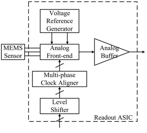
Source: MPDI
AnySilicon connects companies with experienced ASIC design partners capable of developing custom sensor interface and readout ICs, from initial architecture and feasibility studies to silicon validation and volume production.
Describe your requirements and let AnySilicon help identify suitable design partners.
A sensor interface ASIC is a custom integrated circuit that converts signals from a sensing element into information that an electronic system can process.
Many sensors produce extremely small analog signals, sometimes in the microvolt or millivolt range. These signals often require amplification, filtering, compensation and analog-to-digital conversion before they can be used.
A sensor interface ASIC may integrate several functional blocks:
Integrating these functions into a dedicated chip can reduce external component count and optimize the complete signal chain for the sensor’s characteristics.
A readout IC (ROIC) performs a related function, acquiring and conditioning signals from a sensor or detector, sometimes across many parallel channels. The required architecture depends on the sensor technology, signal levels, bandwidth and readout requirements.
Custom sensor interface and readout ICs are used across many industries.
| Application | Typical ASIC Requirements |
|---|---|
| Industrial pressure sensors | Low-noise amplification, temperature compensation, ADC |
| Medical and biosensors | Low-power analog front ends, high input impedance |
| MEMS accelerometers and gyroscopes | Capacitive sensing, filtering, calibration |
| Magnetic and Hall sensors | Position measurement, offset compensation |
| Temperature sensing | Precision references, low offset and drift |
| Industrial data acquisition | Multichannel ADCs, programmable gain |
| Optical sensors | Transimpedance amplifiers, detector readout |
| Gas and chemical sensors | Low-current measurement, sensor excitation |
| Robotics and automation | Sensor fusion interfaces, position and motion sensing |
| Imaging and detector arrays | Multichannel readout, synchronization, low-noise signal acquisition |
For example, an industrial pressure sensor manufacturer may require a custom mixed-signal ASIC integrating a programmable instrumentation amplifier, a high-resolution ADC, temperature compensation and a digital communication interface.
A custom implementation could eliminate several external components while enabling calibration tailored to the sensing element.
A sensor interface ASIC generally combines analog and digital subsystems:
Sensor → Input Protection → Analog Front End → ADC → Digital Processing → Communication Interface
Additional blocks may include calibration memory, sensor excitation, power management, clock generation and diagnostic circuitry.
The analog front end is particularly important because errors introduced at the input cannot always be removed through subsequent digital processing.
Depending on the application, designers may use chopper stabilization, auto-zero techniques, differential architectures or correlated double sampling to reduce offset and low-frequency noise.
ADC architecture is another important decision. Sigma-delta converters are frequently considered for precision, relatively low-bandwidth sensing, while SAR converters can offer an attractive balance of resolution, sampling speed and power consumption.
The best architecture depends on the complete system specification rather than ADC resolution alone.
FIND SENSOR ASIC DESIGN PARTNERS – GET 3 QUOTES
Before approaching an ASIC design company, it is useful to define the main electrical and commercial requirements.
The following table illustrates specifications for a hypothetical precision industrial sensor ASIC.
| Parameter | Example Design Target |
|---|---|
| Sensor input | Differential, 0–20 mV |
| ADC resolution | 16–24 bits nominal |
| Input-referred noise | Below 1 µV RMS |
| Number of channels | 1–8 |
| Sample rate | 100–10,000 samples/second |
| Supply voltage | 1.8V / 3.3V |
| Digital interface | SPI or I²C |
| Operating temperature | −40°C to +125°C |
| Semiconductor technology | 180nm or 130nm CMOS |
| Packaging | QFN or other suitable package |
These values are illustrative design requirements, not guaranteed performance or a specification for an existing product.
An experienced ASIC design partner should evaluate system-level accuracy, noise bandwidth, effective resolution, power consumption, channel matching and calibration requirements before selecting an architecture.
Sensor interface ASICs are often implemented using mature CMOS and mixed-signal semiconductor processes.
| Technology Node | Potential Applications |
|---|---|
| 350nm | Precision analog and selected high-voltage applications |
| 180nm | Analog front ends, sensor conditioning, mixed-signal ASICs |
| 130nm | Sensor interfaces, ADC integration, embedded control |
| 90nm / 65nm | Mixed-signal ICs with increased digital integration |
| 55nm / 40nm | More digitally intensive sensor-processing SoCs |
A smaller technology node is not automatically better.
For precision analog sensing, factors such as device noise, matching, input-voltage range, available analog components and process maturity can be more important than transistor density.
The availability of suitable ADC IP, embedded nonvolatile memory, high-voltage devices and sensor-specific modules must also be evaluated.
Technology availability differs between foundries and specific process variants.
The cost of developing a sensor interface ASIC depends on its complexity, technology, performance specifications, design reuse, manufacturing requirements and qualification level.
The largest initial expense is generally non-recurring engineering (NRE), including architecture development, circuit design, verification, layout and engineering validation.
| Project Scope | Planning Budget (USD) |
|---|---|
| Feasibility study and ASIC architecture | $20,000–$75,000 |
| Relatively simple sensor interface ASIC | $200,000–$600,000 |
| Complex multichannel mixed-signal ASIC | $600,000–$1.5 million |
| Advanced or heavily qualified sensor SoC | $1.5 million+ |
These are broad, illustrative planning allowances, not published supplier quotations or validated industry price averages. The scope covered by each estimate must be agreed with the design partner. Prototype fabrication, packaging, testing, third-party IP, qualification and additional silicon revisions may be charged separately.
Multiproject wafer (MPW) services allow several ASIC designs to share manufacturing resources, reducing initial prototype fabrication costs.
For example, the published EUROPRACTICE 2026 pricing schedule includes:
These are examples of published standard prototype-fabrication charges under specific conditions, not complete ASIC development prices. Process options, design area, eligibility, packaging and other services affect actual costs.
REQUEST A SENSOR ASIC DESIGN COST ESTIMATE
A full custom mixed-signal ASIC program can take approximately 18–24 months from initial concept to production-ready silicon, depending on complexity, foundry availability and qualification requirements.
A representative project schedule is shown below.
| Project Phase | Indicative Timeline |
|---|---|
| Requirements and feasibility | Months 1–2 |
| Architecture and technology selection | Months 2–4 |
| Analog/digital design and simulation | Months 4–9 |
| Layout, verification and signoff | Months 8–11 |
| Tapeout, wafer fabrication and packaging | Months 11–16 |
| Silicon characterization and validation | Months 16–19 |
| Qualification and production preparation | Months 19–24 |
Phases may overlap. This is a planning example, not a committed delivery schedule. A silicon redesign or additional qualification can extend the program.
During development, the ASIC design team typically performs schematic design, analog simulation, process-voltage-temperature corner verification, Monte Carlo analysis, layout matching analysis, parasitic extraction and physical verification.
Following fabrication, engineers verify performance across voltage, temperature and operating conditions. Production test coverage, calibration procedures, reliability and manufacturing yield are also important considerations.
A custom sensor ASIC generally requires higher upfront development investment than an off-the-shelf IC solution.
However, the investment may become attractive when the ASIC significantly reduces component cost, PCB area, assembly complexity or power consumption.
Consider an illustrative project:
| Parameter | Example |
|---|---|
| ASIC development investment | $500,000 |
| Annual production volume | 100,000 units |
| Product lifetime | 5 years |
| Total production volume | 500,000 units |
| Amortized development cost | $1.00 per IC |
| Assumed recurring system cost saving | $2.00 per unit |
| Potential gross savings before NRE | $1 million |
In this simplified scenario, a $2.00 recurring saving across 500,000 units provides $1 million in total savings before subtracting $500,000 in development investment.
Actual economics must also include wafer cost, yield, packaging, testing, inventory, financing, redesign risk and the opportunity cost of development time.
The business case should therefore be established before committing to a custom ASIC program.
Selecting the right ASIC design company is critical, particularly for precision analog and mixed-signal projects.
Key evaluation criteria include:
AnySilicon helps companies identify design partners with relevant expertise rather than approaching multiple suppliers individually.
Yes. Depending on the architecture, an ASIC can support multiple analog input channels, with dedicated or shared amplifiers, ADCs and calibration functions. The optimal approach depends on noise, sampling-rate and channel-isolation requirements.
Often, yes. Many precision analog and mixed-signal designs benefit from mature CMOS technologies. However, the best process depends on sensor performance, power, available IP and manufacturing requirements.
Yes, provided the architecture is suitable for integration. A feasibility study should evaluate which external components can be integrated, expected die area, development costs and potential per-unit savings.
AnySilicon connects customers with semiconductor design companies offering services that may include architecture, ASIC design, physical implementation, tapeout, packaging, testing and production support. The exact scope depends on the selected supplier.
Whether you are developing an industrial sensor, medical device, MEMS product or custom measurement system, selecting an experienced design partner is an important first step.
AnySilicon can help you find suitable ASIC design companies for your technical requirements, project budget and development schedule.
Submit your project requirements and receive information about relevant design partners. The initial quotation request is free, and you can choose how to proceed.
GET 3 SENSOR ASIC DESIGN QUOTES
Start your custom sensor ASIC project with AnySilicon.