

Clock tree synthesis (CTS) plays an important role in building well-balanced clock tree, fixing timing violations and reducing the extra unnecessary pessimism in the design. The goal during building a clock tree is to reduce the skew, maintain symmetrical clock tree structure and to cover all the registers in the design. We have captured some problematic scenarios and the problem solving approaches in this article.
Clock tree network enables in making design clean from a timing perspective. However, it is responsible for more than one third of the total power consumption of the chip. The impact of variations in the clock path is more than 2 times the other paths in the design. These variations in-turn affects the timing paths. Let us take an example; Due to the variation, if the clock path to the launching register is slowed down by 100ps and the clock path to the capturing register is fastened by 100ps then it impacts the setup constraint by adding 200ps more to it, this in-turn affects the timing path by making it more critical. Here we can see the importance of building a balanced clock tree. We will discuss on the timing improvements and methods to reduce the variations in the clock tree. The steps followed in building a customized clock tree and the steps followed to bring down the variations in the clock tree has been depicted in the following sections.
1. Addressing design challenge of registers placed far apart
The section describes the problem encountered and fixes while building the clock tree when registers are far apart. Referring to the diagram (Figure-1) below the clock port is positioned at the middle of the bottom part of the chip. The encircled part at the bottom of the chip represents the digital glue logic that is communicating with the digital logic (beside analog block) at the top of chip. There are large magnitude of setup violations observed on these paths. Being a full chip design, the output delay was critically constrained that led to large timing violations on the output pads. Here are some methods targeted to meet setup timing by building a customized clock tree.

Automatic clock Tree Synthesis Technique
With Automatic clock tree synthesis, the CTS engine puts a lot of buffers across the chip that are not desired. The registers near the clock port face large insertion delays. This effect is due to the clock balancing nature of automated CTS engine. The Clock tree structure will be H-tree similar to the figure-1. Since the chip size is large, the number of buffers are huge on the clock tree due to clock balancing. This renders the experiment not to be useful.
Macro Modeling Technique
With macro modeling method, the target is to add insertion delay to the clock pins of specific registers in order to meet reg2reg timing paths. Let us take an example; consider a path between launch register (Bottom digital logic) and capture register (Top digital logic) as shown in Figure 1. Since the path is long, the setup time was failing with a value of – 3ns in a clock period of 10ns. The target was to insert skew of 3ns on the capture path of the register. However, the issue with this technique was that the paths originating from the capture register were getting affected by 3ns insertion delay. This experiment degraded the timing further due to cascading effect.
Cloning Technique
With respect to figure-1, there is a register (bottom digital logic) that is communicating to registers in 16 digital logic’s (Top digital logic). Here the idea is to clone the register (bottom digital logic) on the three sides (top, left and right) of the chip to improve timing on the affected paths. The method was proposed to the RTL designers to change the logic to put four registers instead of one. Requirement was, no logical cells could be placed in the Soft Blockage region and in between the Analog blocks hence, this method was not effective.
Building Customized Clock Tree Technique
The technique included building clock tree separately for the registers situated far from the digital logic (at the bottom); this helped avoid extra insertion delay for the registers that were near to the clock port. This brought down the buffer count thereby reducing the extra pessimism. The paths between bottom digital logic and top digital logic were pipelined since the paths received clocks at different timings due to different clock tree. Within the top digital logic, no timing violations were encountered since the logic was receiving the same clock. Another benefit of this experiment was, the registers communicating to the output pads also had a separate clock tree, due to this desired latency figure on the launch clock path was entered so that the setup window got relaxed for the Reg2Out timing paths.
Steps followed
This technique enabled meeting timing requirements for the mixed signal chip.
2. Working with High Frequency Designs
A Design had an operating frequency of 6Ghz. The challenge was to make the design operate at 6GHz that was not supported by the standard cells (library’s maximum operating frequency limit was 3 GHz). The clock was divided into 1.5 Ghz to support library’s maximum operating frequency with the help of RTL. The idea was to launch and capture the data four times (to meet 6 Ghz timing) in the same clock period (0.666ns/1.5Ghz) with the help of change in RTL code and the clock definition constraint file. This led to creation of four clocks of 1.5Ghz each and their operation was controlled by using MUX/DEMUX.
In RTL, MUX and DEMUX were used to select the clocks for proper launching and capturing of the data. This was done by activating the clocks at specific time intervals. The clock definitions was changed in a way shown in Figure-2. The MUX and DEMUX structure is shown in Figure 3. By applying proper control signals to the MUX and DEMUX respective clock signal got selected for proper operation. The real challenge was for the RTL designers to come up with an idea like this and implementing the same. Meeting timing in less frequency (1.5GHz) as compared to proposed high frequency (6GHz) got eased.
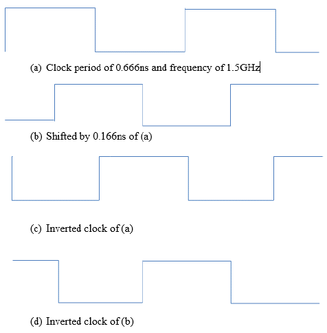
Figure 2
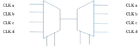
Figure 3
3. Controlling spread of logic
Consider the block in the figure 4(i), the logic is spread across the block and the clock is generated through a different power domain shown in orange, hence there were huge timing violations due to divergence of clock. Due to this clock divergence the derate effect was more. Target was to build a proper clock tree with less divergence so that the derate pessimism is under control.
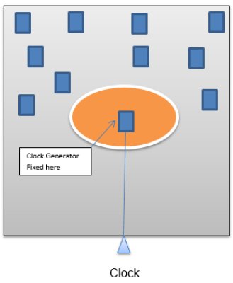
Figure 4(i)
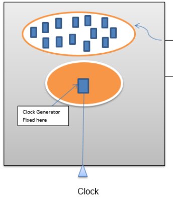
Figure 4(ii)
The idea was to group all the registers together so that the clock tree has less divergence. Hence, the requirement of less pessimism would be achieved in the clock tree. To achieve this, a Region was created for all the registers so that they sit together. This can be seen in figure 4 (ii). After performing the experiment, it is observed that the clock tree was less divergent and timing was much better than before.
Conclusion
The clock tree synthesis and its importance in the physical design flow can be understood from the resolutions discussed above. The importance included the capability of CTS to make the design time clean and bring the clock tree variations down by reducing the buffer count in the design. Various challenges were addressed in tree building stage and the experiments performed yielding results. Clock tree building involves intense effect on the timing and power of the design and hence the clock tree needs to be built with intense care.
This is a guest post by Debaprasad Daxiniray & Chinmaya Masali of Sankalp Semiconductors.


