

Artificial Intelligence (AI) and Machine Learning (ML) have emerged as transformative technologies, revolutionizing numerous industries across the globe. The realm of electronic design automation (EDA) has also been revolutionized by artificial intelligence and machine learning. EDA plays a crucial role in the modern world, as it is responsible for designing the complex circuits and chips that power our electronic devices. AI and ML have made it possible to automate some of the most challenging tasks in chip design, such as layout optimization and circuit synthesis, thereby ushering in a new era of innovation and efficiency. This article explores the rich history of AI and ML, their wide-ranging applications, and their promising future in EDA.

EDA tools are widely used in the semiconductor industry to design chips that are smaller, faster and consume less power. The process of designing a chip involves several stages including circuit design, simulation, verification, layout optimization and fabrication, Each stage is complex, time-consuming and requires skilled engineers with expertise in various domains.
With the advent of AI and ML technologies, EDA tool vendors have developed new solutions that can help automate some of these tasks. These tools leverage vast amounts of data generated during the chip design process to learn from past designs and improve future ones.
In this part of this article, we discuss AI related applications in chip design have been proven to work and are in EDA companies development roadmap.
AI and ML techniques have enabled significant advancements in design optimization and exploration. They can efficiently search through vast design spaces, identifying optimal chip architectures, layouts, and parameters. These technologies assist in reducing design cycles, improving performance, and optimizing power consumption.
ML algorithms have been employed to automate and optimize the physical design and layout of chips. They can analyse and optimize placement, routing, and floor planning, leading to improved performance, reduced power consumption, and faster time-to-market.
Layout Automation: AI can be used to generate automated layout for the physical design of a chip. Layout optimization involves placing standard cells and hard macros in a given floorplan to minimize power consumption while maximizing performance. Traditionally, this has been done by human designers using trial and error methods where they analyse a given floorplan, identify issues and list possible ways a given floorplan can be improved to try as one or more experiments. They do this over many iterations till they achieve satisfactory results. The AI algorithms can be trained on vast amounts of data from previous designs, and the layouts can be optimized much more quickly, accurately and efficiently.
Routing Congestion Prediction and Mitigation: AI can be used to identify routing congestion hotspots early in the design cycle and propose changes to the recipe to mitigate the congestion issues in the design. In the traditional approach, designers would run through place and route multiple times and attempt to fix the congestion following an iterative approach. AI can help reduce the iterations and facilitate faster design convergence.

AI powered EDA tools also help reduce errors during the verification process by checking for inconsistencies between different parts of the chip design automatically. This reduces the time spent verifying designs manually while also increasing accuracy. AI and ML find applications in verifying and testing complex chip designs. They assist in identifying potential design flaws, predicting and mitigating failures, and enhancing the reliability and quality of chips. ML algorithms can analyse vast amounts of data, including simulation results and historical testing data, to improve testing methodologies and speed up the validation process.
Yield Enhancement and Manufacturing: AI and ML are revolutionizing the manufacturing process by enhancing yield rates and reducing defects. These technologies can identify patterns in manufacturing data, predict and mitigate failure modes, and optimize process parameters to improve yield and reduce production costs.
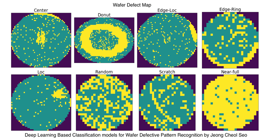
Defect Detection: AI can analyse volumes of manufacturing data, including wafer images and identify patterns associated with defects. By training the labelled defect samples, AI models can learn to accurately classify and detect defects. This enables early detection and prompt corrective actions, reducing the number of defective chips and improving yield.
Process Optimization: AI algorithms can optimize the manufacturing processes by analysing data from various stages, such as lithography, etching, deposition, and packaging. By identifying process variations and their impact on yield, AI can suggest adjustments to optimize parameters like temperature, pressure, chemical concentrations, and timing, ensuring consistent and reliable chip production.
Root Cause Analysis: When defects occur, AI can help identify the root causes by analysing manufacturing data and correlating it with defect patterns. By uncovering the underlying factors contributing to defects, AI can provide insights into process variations, equipment malfunctions, or material issues. This information can guide process engineers in addressing the root causes and improving yield.
Predictive Maintenance: AI can monitor equipment and sensor data in real-time to detect anomalies and predict equipment failures. By analysing historical data, AI models can identify patterns and indicators of impending equipment malfunctions. Early detection of equipment issues allows for timely maintenance and reduces the risk of yield loss due to equipment failures.
Yield Prediction and Optimization: AI can predict the yield of chips by analysing a wide range of data, including process parameters, environmental conditions, equipment status, and historical yield data. By training on historical data and considering various factors, AI models can estimate the yield of current manufacturing batches. This information helps optimize production planning, resource allocation, and process adjustments to maximize yield.
Design for Manufacturing (DFM): AI can assist in optimizing chip designs for better manufacturability and yield. By analysing design data and historical manufacturing data, AI can identify design elements or structures that are more prone to manufacturing issues or yield loss. This feedback can guide designers in making design modifications to improve manufacturability and yield.
Virtual Metrology: AI models can estimate critical parameters or measurements during the manufacturing process without physically measuring them. By using sensor data, process parameters, and historical correlations, AI can provide accurate predictions of important metrics, such as thickness, dimensions, or electrical characteristics. Virtual metrology reduces the need for physical measurements, speeds up the process, and reduces yield loss due to measurement errors.
Circuit synthesis involves generating a circuit from high level specification or description. This task requires considerable expertise in both hardware design and computer programming. AI and ML techniques are leveraged in circuit design and optimization, aiding in the creation of high-performance and energy-efficient designs. They can automate the process of creating analog and digital circuits, optimize circuit parameters, and accelerate the exploration of new design alternatives.
AI can play a significant role in power optimization for chips by employing various techniques and approaches. Here are a few ways AI can assist in power optimization:
Power Modelling: AI can help in developing accurate power models for different chip components and subsystems. By training on large datasets, AI models can understand the power consumption patterns of various operations and predict the power requirements of different chip configurations accurately. These models can guide chip designers in making power-conscious design choices.
Intelligent Power Management: AI can aid in dynamic power management by continuously monitoring the chip’s workload and adjusting power settings in real-time. Machine learning algorithms can analyse the workload patterns and optimize power allocation to different components or subsystems accordingly. This adaptive power management ensures that power is allocated efficiently based on the specific requirements at any given time.
Voltage and Frequency Scaling: AI algorithms can optimize voltage and frequency scaling techniques to find the most power-efficient operating points for a chip. By considering factors like workload, performance requirements, and power constraints, AI can determine the optimal voltage and frequency settings for different chip components, allowing for power savings without sacrificing performance.
Runtime Power Optimization: AI can continuously analyse the chip’s runtime behaviour and identify power-hungry operations or modules. By understanding the relationships between different tasks and their power consumption, AI algorithms can suggest optimizations such as task scheduling, workload balancing, or algorithmic modifications to minimize power consumption during runtime.
Power-Aware Compilation: AI techniques can be used to optimize the compilation process of software or hardware description languages to generate power-efficient code or circuit designs. AI models can analyse code patterns, identify power-intensive operations, and suggest optimizations during the compilation process to minimize power consumption.
Thermal Management: AI can help in thermal management by predicting chip temperature profiles based on power consumption patterns and environmental conditions. By using this information, AI algorithms can optimize power allocation and thermal management strategies to prevent overheating and thermal throttling, ensuring optimal performance and power efficiency.
Voltage drop estimation is a critical signoff check to ensure that the dynamic voltage drop and the static voltage drop are within the spec. The voltage drop issues on the silicon can cause performance loss, excessive heat dissipation, timing errors or even affect the overall functionality of the chip. The simulations for dynamic voltage drop are quite expensive in terms of the compute resources, high cost of sophisticated software tools to run the simulations and even finding the right set of functional and scan vectors for the simulations. Researchers have proposed various machine learning algorithms to predict voltage drop hotspots without running these expensive simulations and to make corrections to the design implementation to mitigate the voltage drop issues early in the design cycle.

Overall, AI can provide valuable insights and decision-making capabilities to power optimization for chips, enabling chip designers to create more energy-efficient and power-conscious designs.
In this part of the article, we discuss AI benefits that are at early stages of research and would need time to mature into a product that is marketable.
Deep learning, with its ability to handle complex and unstructured data, will continue to be a driving force in EDA. Further advancements in neural network architectures, algorithms, and training techniques will enable more accurate predictions, faster convergence, and improved design optimizations.
As AI and ML algorithms become more sophisticated, there will be a growing focus on explainable AI and interpretable models in EDA. Understanding the decisions made by AI systems and providing designers with insights into the design space exploration process will be crucial for their acceptance and trustworthiness.
The demand for AI and ML applications in EDA will drive the development of specialized hardware accelerators tailored for AI workloads. Customized chips and architectures optimized for AI inference and training will provide significant performance gains and energy efficiency improvements.
EDA will increasingly integrate domain-specific knowledge into AI and ML algorithms. By leveraging expertise from chip designers, manufacturing engineers, and domain specialists, AI systems can effectively navigate the complex challenges of chip design and manufacturing.
The future of EDA envisions autonomous design systems that can automate various stages of the chip design process. From initial concept exploration to physical design and verification, AI-powered systems will collaborate with human designers, significantly reducing time-to-market and enhancing overall productivity.
The history of AI and ML showcases their transformative power, leading to breakthroughs in various fields. In the realm of EDA, these technologies have already made a significant impact, revolutionizing design optimization, layout, verification, testing, and manufacturing. With ongoing advancements, the future of AI and ML in EDA holds immense potential for further innovation, efficiency, and automation, paving the way for the next generation of chips and electronic devices.
References:


