

Power, performance and area (PPA) are three core competencies on which an ASIC design is evaluated. In an ideal world, ASIC designers strive to improve the performance of their design in a minimum possible silicon area with lowest possible power dissipation. However, there exists a trade-off between these three key metrics which designers would need to gauge and choose a sweet spot which satisfies the requirements of the given application.
In the past 2 decades, with advent of mobile devices like cellphones, tablets, laptops, smart watches etc., power has taken the center stage in ASIC design. Low power design is critical from many standpoints- some obvious and some non-obvious ones:
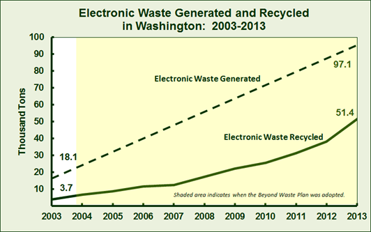
Figure 1: Increase in electronic waste generated over years. Image Courtesy: Washing State Dept. of Ecology
Today, ASIC designers use a plethora of techniques to reduce their power dissipation, and we would discuss them in detail. It would, however, be prudent to first talk about various type of power dissipations and how they trend with technology scaling.
Dynamic power is dissipated in circuits when one of more transistors within the standard cell are switching from either high to low, or low to high. When the integrated circuit is working at “full throttle” which may be while running the most resource intensive application where in a significant or majority portion of the chip is switching states actively, dynamic power dissipation is usually the highest. It may be sub-divided into switching power and internal power.
Switching Power – The amount of switching power dissipated in a circuit is a function of switching frequency, the node capacitance and the operating voltage of the standard cells. This can be minimized by reducing the switching activity, with or without a reduction in the operating frequency, decreasing the node capacitance that’s been charged or discharged, and by reducing the operating voltage. Switching power is calculated as follows:
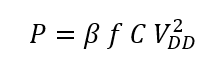
Where ß is the rate of switching, f is the operating frequency, c is the node capacitance and VDD is the operating voltage.
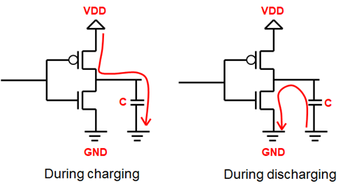
Figure 2: Switching power dissipated while charging and discharging of output capacitance
Internal Power – The component of dynamic power that is dissipated during circuit switching when both pull-up network and the pull-down network are ON intermittently is referred to as internal power. Internal power is directly dependent on the voltage and node capacitance, while indirectly dependent on the node transition. Slower transition times increase the internal power dissipated in the circuits.
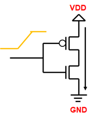
Figure 3: Short circuit power dissipated when both PUN and PDN are ON.
Leakage power is dissipated in circuits when none of the transistors within the standard cell are switching and the inputs are in a steady state. This component of power has become significant in the sub-micron technology processes. It is dependent on the ambient temperature, the threshold voltage of standard cells and the input combination of the standard cell during steady state. Leakage power increases exponentially with an increase in ambient temperature.
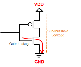
Figure 4: Gate leakage and Sub-Threshold leakage
The goal of designers is to reduce the overall power dissipation of their device- which means reducing the dynamic power during peak performance or by reducing redundant switching when the circuit is not active. Similarly, designers strive to reduce the leakage power of their device when the circuit is in a steady state. There are many techniques used to achieve this.
Switching power has a direct dependence on the operating frequency. When operating in full-throttle mode, the operating frequency is typically very close to the specified frequency, however, this would mean that the chip is burning maximum dynamic power as well. When you are not operating in the full throttle mode, it is possible to scale down the frequency- with or without scaling the operating voltage. This helps reduce the switching power dissipated in the circuits. For example, many commercial CPUs today are able to change the operating frequency depending on the workload.
Since voltage has a quadratic dependence on the switching power, it is most beneficial to scale down the voltage accompanied with scaling down the operating frequency to reduce switching power. This technique is referred to as Dynamic Voltage and Frequency Scaling. When you operate at a lower voltage, the devices get slower. In order to meet timing, one needs to operate at a lower frequency. There are many complexities that designers need to deal with in order to implement DVFS.
By employing DVFS, designers might be able to get away without employing an active cooling mechanism (like use of fans) to reduce the heat generated by the electronic components. DVFS is not restricted to mobile technology arena. Many other applications like automotive SoCs, desktops, servers etc. also employ dynamic voltage and frequency scaling.
Clock signal has the highest toggling frequency of all signals in the design, with a toggle rate of 2.0 because it toggles twice per clock cycle. Consequently, dynamic power dissipated in the clock network accounts for 60—70% of the total switching power dissipated in the circuits. In addition to switching power dissipated in the clock tree network, sequential devices like flip-flops also dissipate a significant amount of internal power. It is therefore prudent to gate the clock when a certain portion of the chip is not active to save on the switching power. This is accomplished using a bunch of architecturally placed clock gates referred to as clock gating integrated cells (CGICs).
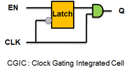
Figure 5: Clock Gating Integrated Cell
Clock gating is perhaps the oldest and the easiest method to save on dynamic power. Modern ASICs use many levels of clock gating to control the granularity of the design that is clock gated.
While clock gating helps reduce the switching power, power gating is useful to reduce the leakage power. As mentioned earlier, leakage power is dissipated during steady state where a small amount of leakage current flows through the transistor substrate to the ground. Power gating cuts off the voltage supply to the standard cells, and therefore limits the leakage power. This can be thought of as similar to standby mode in modern CPUs where a majority portion of the CPU goes to sleep, and only basic housekeeping and critical operations are kept awake to save on the battery life.
Figure 6: ASIC sub-divided into multiple power domains
There’s some penalty that designers need to pay when they employ power gating.
Bigger cells dissipate higher switching power. For all the cells along a timing path with positive slack, it might be possible to opportunistically downsize the cells to recover dynamic power. This is usually accomplished using modern EDA tools, and brings about an incremental change while operating in the ECO (Engineering Change Order) mode. The savings achieved by downsizing would be nowhere close to any of the savings achieved by using one or more architectural methods discussed above.
Many flavors of CMOS and FINFET devices are manufactured which differ in their threshold voltage.
Similar to downsizing, it is also possible to swap the cells with lower threshold voltage to cells with higher threshold voltage to save leakage power, but only in an ECO mode.
During the 90s during the desktop PC era, most of the efforts were concentrated on extracting the best performance out of the design. However, in past decade mobile devices like cellphones, tablets, smart watches and fitness tracking devices have shifted the momentum towards power. Low power is a key for design success. Ever increasing cell integration densities and increasing leakage with shrinking technology has made power optimization one of the most challenging problems that designers have to deal with. The architectural and design techniques discussed in this post are dispensable for designers to help meet their power targets.


