

The semiconductor industry went through several stages of evolution, beginning with the Metal Oxide Semiconductor (MOS) Field-Effect Transistor (FET) which was first proposed by Lilienfeld and Heil in the 1930s, moving on to bipolar in the 1950s and N-channel metal-oxide semiconductor (NMOS) in 1970s, and ultimately becoming the standard in the 1980s with complementary metal-oxide semiconductor (CMOS). Digital circuit applications faced a notable performance gap between bipolar and CMOS logic as depicted in Figure 1 which underscored that neither CMOS nor bipolar technology possessed the flexibility necessary to cover the entire delay-power area.
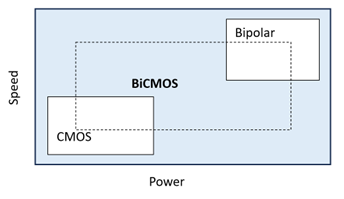
Figure 1. Speed and Power Comparison of CMOS, bipolar, and BiCMOS technologies
BiCMOS emerged in 1983 as a result of the constant research and development of new technologies driven by the need for greater performance which fabricated CMOS and bipolar a single integrated chip, to exploit their advantages and compensate for each other’s shortcomings at the circuit and system level. The conventional practically used BiCMOS circuit as shown in Figure 2 was proposed by Lin et al.
Since 1985, BiCMOS technology has developed beyond the experimental phase to be widely used in production processes. The cutting-edge architectures of bipolar and CMOS converged such that today BiCMOS has emerged as one of the leading technologies employed for high-speed, low-power, and highly functional Very-Large-Scale-Integration (VLSI) circuits, particularly when the BiCMOS process has been refined and integrated into the CMOS process with no extra steps. The process steps can be effectively shared for both bipolar disorder and CMOS because the process steps needed for both conditions are comparable.
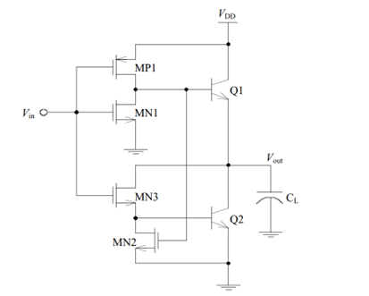
Figure 2. Conventional BiCMOS Inverter
The following are the semiconductor foundries that provide access to BiCMOS process technology
BiCMOS integrated Circuit fabrication process, as shown in Figure 3, encompasses several fabrication steps which may differ depending on the manufacturing facility [6].
Step 1: The process commences from a semiconductor substrate preparation, primarily of silicon, and undergoes thorough cleaning for eradication of impurities and contaminants.
Step 2: Subsequently, a thin epitaxial layer is deposited onto the substrate to enhance the device’s electrical properties and overall performance.
Step 3: Next, a metal oxide layer (SiO2) is deposited on the substrate’s surface to provide electrical insulation between various layers and chip components.
Step 4: Photolithography is performed involving the application of photoresist material to the metal oxide layer and placing a photomask containing the required circuit patterns over the substrate. The ultraviolet light employed for exposing the photoresist through the photomask transferred the circuitry patterns to the chip.
Step 5: Through chemical etching, the exposed or unexposed portions of the photoresist are removed to effectively transfer the circuitry patterns onto the metal oxide layer.
Step 6: Dopant implantation separates the substrate into p-type and n-type regions through various dopant atoms, resulting in discrete regions for both bipolar and CMOS components.
Step 7: After ion implantation, thermal annealing is performed to activate the dopants that were implanted and repair any potential damage.
Step 8: Then, metal (copper or aluminum) deposition is employed for establishing connections between different chip components.
Step 9: Insulation layer is deposited on top of the metal layers, typically SiO2.
Step 10: Lastly, each chip is tested for functionality, and protection housing is incorporated with connection pins and leads upon verification.
By combining these highly coordinated stages, the BiCMOS integrated circuit fabrication method represents the combination of state-of-the-art semiconductor technologies, resulting in the development of sophisticated semiconductor devices.
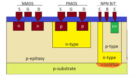
Figure 3. BiCMOS Fabrication Architecture
Modern electronic design has benefited greatly from the revolutionary advantages of BiCMOS technology, which combines bipolar and CMOS technologies. Its ability to smoothly integrate digital and analog signals on a single chip, which makes mixed-signal ICs (Integrated Circuits) possible, is its primary strength. This special feature enables engineers to create complex devices that can combine many signal types into a single architecture.
The capability of this technology includes low propagation delay and high-speed switching, which is essential for applications requiring quick data processing. The development of devices with low power consumption is made easier by the notable energy efficiency of BiCMOS technology, which is an important feature in the current environment that emphasizes energy conservation.
High noise immunity is another feature of BiCMOS devices that guarantee reliable signal processing in interference-prone settings. High packing density provided by the technology allows for the creation of strong integrated circuits (ICs) in small form factors that balance performance and spatial efficiency.
Applications for BiCMOS technology include mixed-signal integrated circuits (ICs) that work with both analog and digital circuits. It encompasses gadgets such as signal processors, communication systems, and data converters. BiCMOS stands out as a fundamental technology in the field of high-speed communication systems, exhibiting both flexibility and dependability.
BiCMOS is ubiquitous in wireless technology, contributing to Bluetooth, Wi-Fi, radio frequency circuits, and wireless sensors, among other non-conventional uses. It is essential to the development of sophisticated systems like engine control and anti-lock braking systems in automobile electronics. Its adaptability across a wide range of applications is further demonstrated by the fact that the technology is driving the development of high-performance data transfer interfaces like USB and HDMI. Essentially, the many benefits of BiCMOS technology highlight its fundamental place in contemporary electronic systems and provide a solid platform for further development.
Answer a few questions and get a recommended shortlist of foundries. Full scoring and a longer shortlist by email.
Integrated circuit design has undergone a paradigm shift with the introduction of BiCMOS technology, especially when it comes to high-speed and low-power capabilities. Traditionally, the use of low-power circuit design was limited to specialized industries like pacemakers and wristwatches because of the high costs and complexity of CMOS and BiCMOS technology. However, due to the critical role that power limits play in modern high-performance applications, the environment has changed, and low-power design has gone from being a specialist endeavor to a universal need. The growth of portable systems, where energy efficiency has become a primary design goal, highlights this shift.
BiCMOS has a remarkably broad range of applications, including radio frequency (RF) systems and mixed-signal integrated circuits. The ability of mixed-signal integrated circuits (ICs) to smoothly combine analog and digital signals on a single chip is essential for creating complex devices that can handle a wide range of signal kinds. BiCMOS performs well in RF systems concurrently, which helps to improve signal processing and communication capabilities.
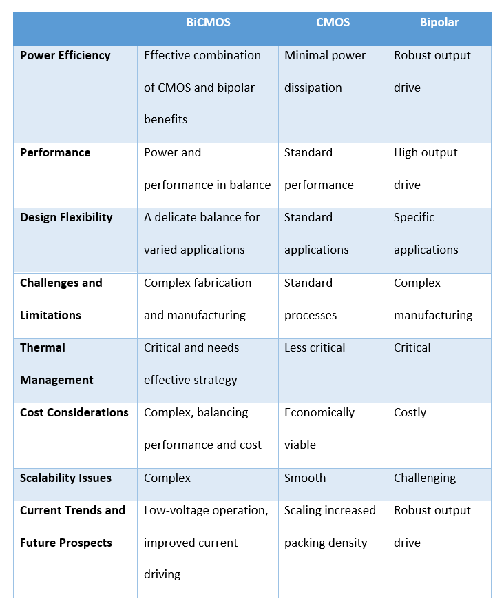
BiCMOS dominance in the semiconductor industry is further strengthened by its advantages in power management and analog front-end designs. The size, weight, and frequency of recharging of battery packs become critical variables as portable systems become increasingly important. In order to ensure both portability and energy efficiency, BiCMOS technology offers a careful balance between high packing density and low power dissipation [12]. BiCMOS stands out as an appealing option when compared to other semiconductor technologies because it combines the high packing density and low power dissipation of CMOS with the high output drive speed and high speed of bipolar devices. BiCMOS is positioned to be a leader for years to come due to its ability to handle the demands of modern electronic systems, which include decreasing power and voltage requirements, as well as the growing need for device downsizing. Table 1 provides a concise comparison, highlighting the diverse spectrum of semiconductor technology, with BiCMOS showing immense potential.
Table 1. Comparison of BiCMOS and Other Technologies
Adoption of BiCMOS has challenges even though it offers a potential confluence of CMOS and bipolar benefits. BiCMOS’s hybrid nature makes fabrication and manufacturing procedures more complex, requiring cutting-edge technological capabilities. An important issue that arises is thermal management, requiring efficient methods to reduce heat generation and guarantee circuit stability. BiCMOS technology integration requires a careful balance between economic feasibility and performance advantages due to cost and scalability constraints.
BiCMOS continues to establish itself in the rapidly changing field of semiconductor technology. Present developments highlight the pursuit of better device features by means of low-voltage operation and enhanced current driving capabilities. A common trend to achieve high-speed, low-power consumption, and improved packing density is a shift towards smaller dimensions, shown by scaling [13]. BiCMOS is notable for its ability to integrate an entire system onto a single chip, which offers enormous power savings. Substrate engineering will probably be essential in the future for maintaining low threshold voltages, which will solve a significant device issue related to simple scaling.
Within the BiCMOS technology framework, SiGe heterojunction bipolar transistors (HBT) have spread throughout many industries, finding use in optical data lines, high-precision analog circuits, automobile radar, and high-speed wireless communication. Although 5G communication standards utilizing cutting-edge CMOS technologies are soon to be released, SiGe BiCMOS stands out as a strong competitor, especially when it comes to meeting the increasing needs of fiber optic backhaul and high data rate wireless.
Current developments, as demonstrated by the European research project DOTSEVEN, are causing a dynamic evolution of the BiCMOS technology landscape. These include novel mm-wave circuit applications of SiGe HBTs, advanced modeling methodologies, and technological improvements. The continuous improvement of SiGe BiCMOS technologies’ radio-frequency (RF) performance opens the door to highly-integrated millimeter and sub-millimeter wave circuits, which in turn supports applications such as short-range data transfer, robotics, and medical imaging that require high-resolution sensors.
BiCMOS RF capabilities have advanced significantly with the development of a new generation of SiGe HBTs that have peak fT/fMAX values of 505 GHz/720 GHz and Current Mode Logic (CML) ring oscillator gate delays of 1.34 ps. The integration of these high-performance HBTs into an RF BiCMOS platform may lead to significant improvements in terahertz (THz) and millimeter-wave (mm-wave) applications. One important element affecting the RF performance of SiGe HBTs is the scaling of vertical and lateral device dimensions, especially through epitaxial growth of the SiGe base layer stack.
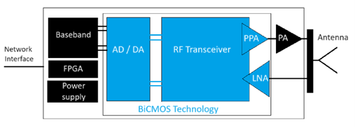
Figure 4. Typical point-to-point radio receiver or cellular base station
The state of the art for high-performance RF ICs is BiCMOS technology. BiCMOS SiGe (Silicon-Germanium) technology provides ideal options for the expanding broadband data market with investments in aggressive R&D. Efficiency is increased when RF, analog, and digital functionalities are combined onto a single chip, greatly reducing the need for additional components. Nowadays, BiCMOS technology is used extensively in wireless base stations, optical transceivers, automotive radars, and instrumentation solutions across the globe, demonstrating its ability to satisfy a wide range of requirements as shown in Figure 4 and Figure 5.
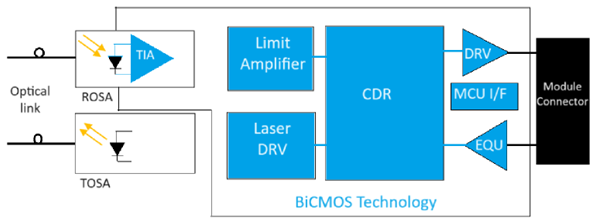
Figure 5. An example of an active optical cable module and optical fiber
SiGe BiCMOS techniques have evolved over the last 20 years beyond what was once thought of as a “niche” technology. They have demonstrated their ability to meet both new circuit demands and the replacement of conventional discrete III-V device technologies by continuously completing crucial gaps in the requirements of commercial semiconductor products [17]. BiCMOS is a cornerstone technology that affects a variety of industries, including high-performance computing, telecommunications, and the automotive sector. This is due to its inherent reliability and flexibility.
BiCMOS is essential to the development of high-performance computing and communication systems because it makes enhanced functionality in electronic devices possible. A major factor in its success has been its flexibility in responding to particular application needs. This has helped it move beyond specialized uses and develop into a flexible and affordable answer to a wide range of semiconductor product needs.
It is clear from examining the development of SiGe BiCMOS technology that its implications and possibilities are extensive. Recognizing its versatility, continuous improvements, and continuous capacity to bridge new applications gaps for semiconductor products are key factors in predicting its future use. SiGe BiCMOS’s journey is one of promise and possibility, and it is expected to play a significant role in defining the semiconductor industry for years to come.
References:
[1] J. E. Lilienfeld, U.S. Patent 1,745,175 (1930).
[2] O. Heil, U.S. Patent 439,457 (1935).
[3] J. Mayamoto, S. Saitoh, H. Homose, H. Shibata, K. Kanzaki, and S. Kohyama, “A 1.0 µm N-Well CMOS/Bipolar Technology for VLSI Circuits,” IEEE IEDM, Tech. Dig., pp. 63–66, 1983
[4] T. Ikeda, T. Nagano, N. Momma, K. Miyata, H. Higuchi, M. Odaka, and K. Ogiue, “Advanced BiCMOS Technology for High Speed VLSI,” IEEE IEDM, Tech. Dig., pp. 408–411, 1986.
[5] J. Miyamoto, S. Saitoh, H. Momose, H. Shibata, K. Kanzaki, and T. Iizuka, “A 28 ns CMOS RAM with Bipolar Sense Amplifiers,” IEEE ISSCC, Tech. Dig., pp. 245– 248, 1984
[6] Embabi, Sherif HK, Abdellatif Bellaouar, and Mohamed I. Elmasry. Digital BiCMOS integrated circuit design. Vol. 193. Springer Science & Business Media, 2012.
[7] https://patents.google.com/patent/US6476450
[8] https://www.elprocus.com/bicmos-technology-fabrication-and-applications/
[9] Puchner, Helmut. Advanced process modeling for VLSI technology. Österr. Kunst-u. Kulturverl., 1996.
[10] https://www.tutorialspoint.com/bicmos-technology-fabrication-process-and
applications
[11] https://www.pearsonhighered.com/assets/samplechapter/0/1/3/0/0130321621.pdf
[12] Machado, Gerson AS, ed. Low-power HF microelectronics: a unified approach. Vol. 8. IET, 1996.
[13] Alvarez, Antonio R., ed. BiCMOS technology and applications. Springer Science & Business Media, 1993.
[14] Zimmer, Thomas, Josef Böck, Fred Buchali, Pascal Chevalier, Michael Collisi, Björn Debaillie, Marina Deng et al. “SiGe HBTs and BiCMOS technology for present and future millimeter-wave systems.” IEEE Journal of Microwaves 1, no. 1 (2021): 288-298.
[15] Rücker, Holger, and Bernd Heinemann. “High-performance SiGe HBTs for next generation BiCMOS technology.” Semiconductor Science and Technology 33, no. 11 (2018): 114003.
[16] https://www.st.com/content/st_com/en/about/innovation—technology/BiCMOS.html
[17] Preisler, Edward. “A commercial foundry perspective of SiGe BiCMOS process technologies.” In 2020 IEEE BiCMOS and Compound Semiconductor Integrated Circuits and Technology Symposium (BCICTS), pp. 1-5. IEEE, 2020.
