

Chip design is a process of designing a chip and is an essential part of electronics engineering. This process of chip design involves the knowledge of circuit design and its logic formation. All chips are made using basic elements which are known as transistors. The Metal Oxide Silicon Field Effect Transistor (MOSFET) is the basic building block of digital chips which is used to make complex circuits.
The history of chip design is linked with the development of transistors. Jack Kilby developed the first integrated circuit in 1958 and it only contained a single transistor. The size of first IC was about 17.76 mm2. The first integrated circuit used Germanium as the semiconductor material. Although Germanium has high electron mobility but still it is almost vanished from the IC industry, but silicon stays as it is the most abundant element in the world.
Initially, this chip was used for military purposed but soon caught the attention of household and healthcare industry. In 1965, Gordon Moore presented a rule where he said that the number of transistors in a chip with a given area will be doubled every 18 to 24 months. This law was intact till late 90s, but with the recent development of reduced size transistors, this law is no longer valid. The number of transistors has reached to multi-billions in a chip.
The modern trends in chip design together with advance EDA tools have made the design of chips more scalable and more reliable than ever before.
The physical size of transistors has decreased enormously over past decade. This led to both very large chip and also a low voltage chip design which means that chips consume very less power, even a few micro-watts of power. This allowed high scalability of chips in various markets and industries both in terms of chip size and market penetration.
The other important trend in the chips design is the use of co-simulation (hardware and software) design. In this way, the whole algorithm is divided in two sub-blocks: (i) the sub modules which require intensive computation are taken to hardware i.e. chips, (ii) the complex modules which are dependent on the data and are involved in decision making are processed on the software. Example below is a good example to show how the design process is divided in different subsets.
Finally, IP cores are very important for chip design process. If whenever a designer has to implement a complex design, he can use IP cores save time and reduce development risk.
Shrinking Transistor Geometries
Hardware–Software Co-Simulation
Reusable IP Cores
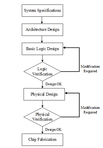
Chip design process is very similar to the FPGA design flow. There is only one difference: chips are manufactured or fabricated after the design is finalized. The chip design flow is shown in figure below.
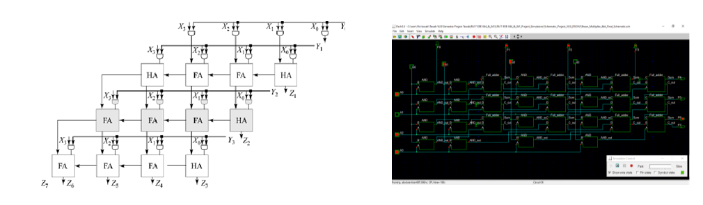
For practical reasons we will use in this article an example of a 4×4 Array Multiplier design which is a digital design.
The first and most important step of the chip design process is defining and creating the specification of the system. The main purpose of the system is to get multiplied 2 4-bit inputs. And the expected result should be about 8-bits wide.
Architecture Design
The next step is to design the architecture of the system where we decide which blocks are going to be used and what hierarchy level this system is going to operate.
Basic Logic Design
After the architecture design, the basic logic system is designed. For the example quoted above, a logic diagram is shown on the left while a schematic design is shown on the right. This schematic is designed using a software tool called DSCH.
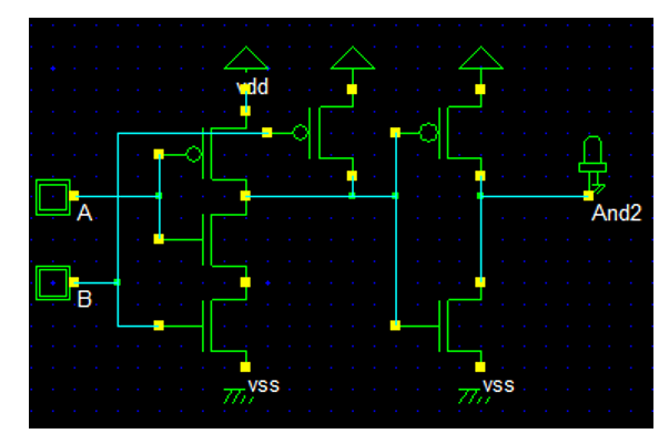
All the modules (AND, Half Adder, Full Adder) which are used to make this multiplier are made from basic transistors. An example schematic of AND gate is shown below. We can see that there are 6 transistors are used in this simple diagram and there are a lot of interconnects as well.
Logic Verification
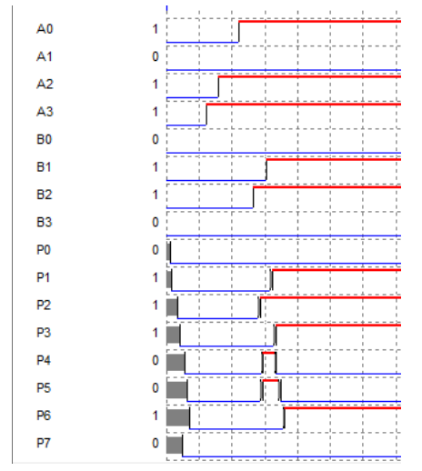
When the schematic design of the system is complete, the next step is to verify the system functionality. This can be done using the simulations in same tool. This step is important, as it will help to verify at the initial level and if any issue is found in the functionality of the system, it can be removed in the start. If any issue is found, then one has to go back to the schematic design level and debug for issues and come up with the updated schematic. The verification waveforms for the above system are shown. Please also note that in complex systems, the simulation and verification of the systems will be a tougher job.
Physical Design Layout
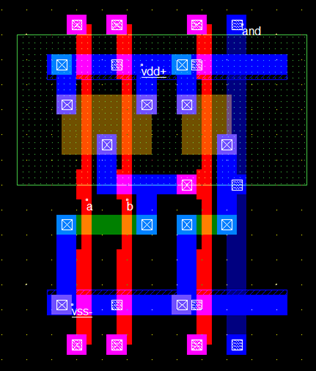
The next and most important step is to translate the system to physical level. At this level, the schematic is converted into physical layout using basic building blocks. For example, the below diagram shows the layout of a two input AND gate which was shown above. We can observe that each transistor is replaced with the corresponding physical layout, while the interconnects are replaced with different metal layers like Metal 1, Metal 2 and Polysilicon. This seems to be a bit complex process, as the designer has to make all the transistors and interconnects by hand.
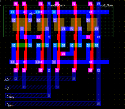
The figure below shows physical layout of the half adder, here one can observe that as the modules are linked together, the process becomes tougher. Because we have to make sure all the transistors are placed properly, the transistors must not occupy un necessary space, all the interconnects are added as per the schematic design, multiple layers of interconnects are used to avoid complexity and all the required contacts are added to make a joint two different layers.
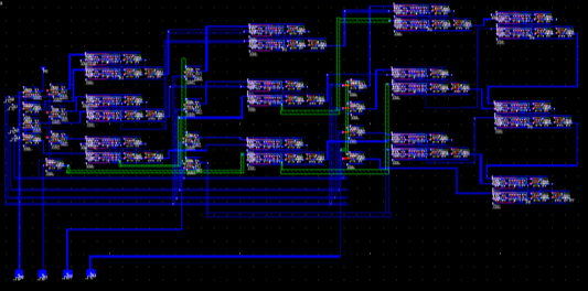
The overall system for the 4-bit multiplier is shown in figure below. One can observe that as the abstraction of the system is decreased, the system becomes more complex.
Physical Design Verification
Before going to fabrication facility, the verification of physical layout is required. For that multiple verification techniques are used including (i) Design Rule Check (DRC) where the designing tool checks for any violations in the design rules, like metal spacing, contact sizes etc, (ii) Layout vs Schematic (LVS) check is used to verify if the layout designed is similar to the schematic design, and checks all the connections and verifies them, and (iii) Timing and Power Analysis is used to verify if the layout made violates any timing issue and adds unnecessary delays, if there is any violation, this can be removed by adding inverters and buffers, where required. Poor planning of timing delays results in lower frequency of operation, so this validation and correction of timing delays is important for any designer. The power analysis shows that how much power the system is going to consume and also it tells at what voltage the system is going to operate.
Fabrication and Final Testing
The final step is the fabrication of the physical layout design. While designing system on the tools, all the libraries and layer information is provided by the foundry which is going to fabricate the chip. After the system is designed and verified, a .GDS file is sent to foundry for fabrication.
The final testing is done on hardware, for that a prototype PCB can be made on which the chip is mounted, and all necessary interfaces are added onto the PCB for testing. For final testing, another important step is to add internal test nodes within the system which are critical to debug the system while testing on actual PCB.
Get a fast indicative cost range, then unlock a full breakdown by email.
There are different companies who offer tools for chip design. For each stage of the design process, the tools are different. The following are two of the major players in the chip design tool market.
Siemens provides various designing and verification tools for IC designing which include: (i) Signal Integrity Analysis to make sure that to reduce the time of designing and making the design perfect in first go, (ii) “Calibre Design Solutions” which is used to overcome the capacitance issues in the circuit and (iii) “Custom IC” for complete . Further details of the software can be accessed at (https://eda.sw.siemens.com/en-US/ic/products/).
Cadence is one of the giants in the IC design industry. They provide tools which can be used to create both Analog and Digital ICs. Cadence also offers very effective tools to reduce the designing burden from the designer by providing auto layout generation tools. In this way a designer creates a top level module in an RTL language and the tool translated it to the physical level. The link for Cadence tools is https://www.cadence.com/en_US/home/tools/custom-ic-analog-rf-design/circuit-design.html.
The two factors which are changing the future of chip design industry are: (i) introduction of single digit nodes (ii) the advancement of design tools. The first is below 10nm silicon wafers which brings new range of high computing chip such as CPU and accelerator to datacenters, this will allow us to have many millions of computing power all around us. So, the second factor supports this development. The modern tools are enabling the designers to overcome the tedious work on physical design process and give them the way to create the chips using automatic design tools, where the designer works on higher level, while the tools transform the higher-level system to physical level design for fabrication. This means faster design cycle of chips.
