

A smaller form-factor with higher data transfer rate, signal integrity, memory bandwidth, and thermal capability are all criteria for improving system performance. Today’s highly integrated and portable products strive to improve all of these metrics. Through Silicon Via (TSV) packaging technology enables homogenous and heterogeneous integration of logic and memory co-located closely together in a small form-factor assembly. The use of copper pillar technology on interposers achieves line and space widths with very fine pitch interconnects and enables high-density signal routing and very high bump counts [1].
In traditional scaling, designers could rely on die shrinks and low core voltage process nodes to keep pace with the need for more bandwidth and computing power. However, the cost of scaling and challenges associated with commercializing very large and complex ASICs is driving the need for radical departures from traditional ASIC and memory implementation into very large systems. Today, TSV technology is being integrated in both memory and logic silicon technologies.
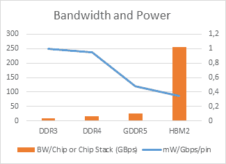
Figure 1. Bandwidth increases and power consumption per Gbps decreases with advanced memory products. (Source: AMD/SK Hynix [2].)
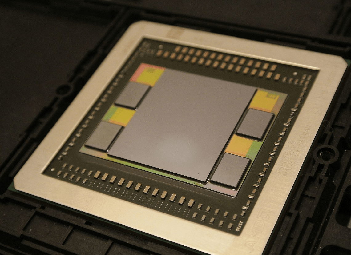
A combination of 2.5D and 3D TSV packaging is shown in Figure 2. All chips reside on a Si TSV interposer. The 3D TSV sits on top of 2.5D TSV and all the dice are adjacent to a very large ASIC GPU. This demonstrates why TSVs provide such an attractive packaging solution. The vertically stacked 3D memory chips significantly reduce board size and routing complexity at the board level. An added advantage of the smaller form factor in the TSV structure is a reduced driver compared to one required for board level or horizontally placed memory chips.
(a)
(b)
Figure 2. A complex system with High Bandwidth Memory (HBM) and ASIC all integrated into a 55-mm FCBGA package. (Image (a) by Kapitaenk [3] and b [4].)
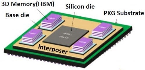
Figure 2 shows how discrete DRAM packages require large board area and long data signals to interface with an ASIC. HBM stacks the DRAM layers vertical, shrinking the foot print significantly and providing high bandwidth with reduced power consumption. When combined with appropriate wafer bumping technology and advanced packaging, TSV interconnects enable very high density I/O so that ASIC and memory die can be located near each other on a TSV silicon interposer. This integration scheme is 2.5D TSV.
Additionally, silicon layers can be stacked tier-to-tier on top of each other, which reduces the physical area allocated for each component. This tier-to-tier stacking is called 3D TSV technology. In the DRAM memory space, 3D TSV has been deployed in both HBM and 3DS. By combining the two TSV technologies into a flip chip ball grid array (FCBGA) assembly, systems with high bandwidth and low power per bit transferred and high memory density are realized.
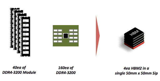
Figure 3. DDR4 vs. HBM Footprint [4].
Interposers for 2.5D are designed to enable side-by-side die interconnect. As such, interposer die sizes are large, sometimes larger than the reticle size. The 2.5D TSVs are generally 100-µm deep to help with die warpage after the wafer is thinned to expose to TSVs on the wafer backside. During the middle-end of line (MEOL) process more bulk silicon will remain, which increases the die resistance to warpage.
In contrast, 3D TSV integration is generally integrated in DRAM with small die area. The 3D TSVs are integrated at 50-µm deep making the die more sensitive to warpage. HBM is built using Chip on Wafer (CoW) molded style assembly technology which does restrict the test coverage available because the memory cube can only be tested while in wafer form. Since HBM test coverage is reduced, it is desirable for 2.5D assembly integration to consider assembly methods that can enable ASIC test before HBM cubes are committed to the assembly process.
When using a CoW molded style assembly, all interposer die sites must be populated before wafer molding. The problem with wafer-level testing is it can only be performed at wafer test sites that are typically limited to how fast the vectors can be run, and parallelism, and even temperature. In contrast, on a substrate using a handler and some form of automation, much higher volume testing can occur with much better test coverage, more I/O on the test board, and more. This provides much more efficient testing at the substrate level. For many customers, this is the right approach today.
2.5D TSV Assembly Technology solutions
Multiple 2.5D TSV technologies have been developed and commercialized to address technology inflection points.
Assembly integration that starts at the substrate level (Chip on Substrate or CoS) readily enables flexible test solutions early in the assembly flow. In contrast, an assembly methodology that begins with a wafer (CoW) will require full population of top die to the interposer wafer and completion of the remaining assembly to a package substrate before suitable testing can begin.
Both CoS and CoW platforms have a unique set of design rules that regulate die-to-die spacing to manage underfill options. Materials used for final assembly can also impact manufacturability. As an example, the CoW process can include wafer-level molding (CoW – Molded), which is used to provide structural rigidity and die protection to the wafer stack for subsequent, down-stream processing and assembly.
A 2.5D TSV CoS process has been in production for several years at Amkor and the CoW process is being qualified in 2016. The process flow details of each of these approaches are shown in Figure 4. For Amkor, the TSV process flow starts with MEOL to expose the foundry-created TSVs and bump the front and back of the wafers to form the interconnects.
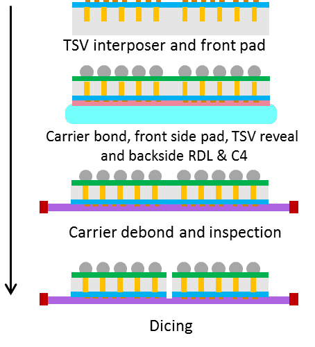
(a) – MEOL Process Flow (CoS)
(b) CoS Assembly Process Flow with Interim Test
Figure 4. CoS MEOL and Assembly w/ Interim Test
Figure 4(a) shows an example of the steps involved with MEOL for CoS. Figure 4(b) shows the CoS assembly steps with interim test step before 2nd top die attach. The MEOL wafer processes are completed delivered to the assembly line for die attach to the PCB. Once the interposer is attached, the ASIC die can be attached. If interim test is desired before HBM attach, the sub-assembly can be tested on an ATE for binning and determine if the sub-assembly can receive the HBM memory. Figure 4(b) indicates testing of the logic + interposer sub-assembly before MEOL testing is completed.
Support for interim test requires the HBM to logic spacing to be large enough to prevent underfill contamination of the HBM die site pads. When planning for interim test this requirement should be considered before finalizing the interposer design.
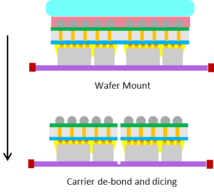
Figure 5 shows an example of the steps involved with MEOL for CoW. This MEOL flow is common between molded and non-molded CoW, so only one MEOL process flow is shown. CoW MEOL differs from CoS in the following ways. Since the die attach step occurs while the interposer is still in wafer form, the wafer carrier must be flipped to the C4 side of the interposer so that the front side of the interposer presented for top die attach.
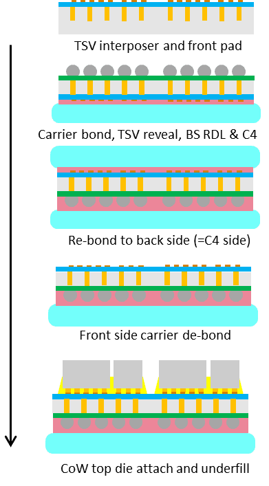
Figure 5. CoW – MEOL (Molded & Non Molded) Process Flow and Die Attach
As mentioned previously, CoW-molded requires the interposer wafer to be fully populated with top die before the wafer over mold process. This is true even for any x-out die sites on the interposer.
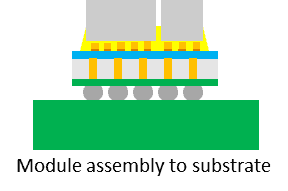
After molding, the wafer finishing includes wafer mold grind to expose the top die for thermal management and to further reduce the volume of mold compound to control warpage and die level stress. This is shown in Figure 6(a). At this time, the wafer can be mounted to a film frame and diced using a mechanical saw. Dicing streets should be designed accordingly. The molded module can then be assembled to the substrate as shown in Figure 6(b). It should be apparent that testing at this point will reveal any yield loss. CoW-molded requires extremely assembly yield to prevent loss of top die. Post-package repair and other DFT schemes should be deployed to reduce risk of yield loss.
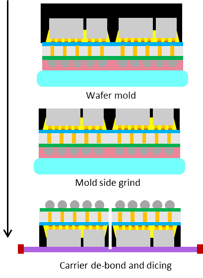
(a) CoW-Molded – Wafer Molding and Thinning
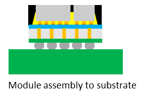
(b) CoW-Molded – Final Assembly to Substrate
Figure 6. CoW – Molded Wafer Finish & Final Assembly
For CoW NoMold, the MEOL process is shown in Figure 7(a). Because there is no wafer molding process, stealth dicing (SD), a laser-based technique, can be used which has design rule advantages as well as very clean die separation. Again, the module can be assembled to a PCB substrate as shown in Figure 6(b).
(b) CoW Module Assembly – NoMold Module
Figure 7. CoW – NoMold Wafer Finish & Final Assembly
The key benefit to the CoW NoMold process is the removal of the mold compound enables logic and memory designs to remain independent and provides good design rule capability for floor planning. Additionally, CoW NoMold does not require full wafer population of the interposer before wafer finish. This is shown in Figure 7(a). As a result, the NoMold module can be diced (using SD) and assembled to a substrate. It should be apparent that this methodology allows for interim test, before the HBM memory device is attached to the interposer.
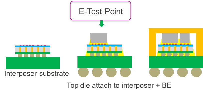
In the CoW NoMold path, an interim test flow (Figure 8, middle) is supported. Die size alignment is not design rule limited, because mold compound is not used in this platform. Furthermore, stealth dicing of the interposer is possible which could reduce the interposer dicing street width. Since the wafer will not be over-molded, every die site on the interposer does not need to be populated. This feature allows for interim test options, either at the wafer-level or at substrate level.
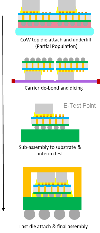
Figure 8. Hybrid CoW+CoS Flow with eTest
TSV Assembly Design considerations
Architects and designers need to understand the nuances between these approaches including the advantages and disadvantages of each. TSV processing whether it is CoS, CoW or even 3D TSV for memory has essentially the same basic approach on the wafer side using a similar MEOL wafer flow. The assembly methodology drives the design rules and test support capability. These are critical tradeoffs that should be considered.
CoS provides the most flexibility. The CoW molded flow has the least flexibility. However, there are two process flows between these extremes. One is the CoW no mold. While it is not as aggressive, it can be modified to perform the hybrid process that combines the best of CoS and CoW.
Table 1 shows a quick high-level summary of several high-level design considerations. There are more criteria depending on the application and specific customer constraints such as improved system performance or high performance at relatively low energy dissipation as measured by bandwidth per unit of energy expended, thermal performance, or others.
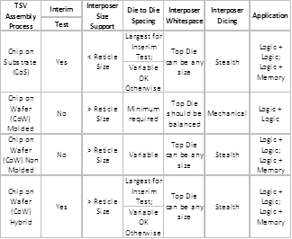
Table 1. TSV Processes and Attributes Comparison
Product test strategy is a major assembly aspect that may determine the choice one process flow versus another. Amkor has been at the forefront of enabling very flexible electrical test, even on partially assembled packages, when it is required. Die yields and test die coverage define the requirement for this capability. By enabling a flexible assembly process flow, interim test can be used to prevent die loss in multi-die MCM packages. The 2.5D logic + memory architectures that use an interim test capable assembly flow can test the logic functionality before committing the HBM dice to the interposer. Some designs call for up to four HBM placements which can be very costly if the logic functionality cannot be verified prior to memory attach.
TSV Design Options
With TSVs commonly accepted as a solution for advanced IC packaging, today’s design decisions focus on identifying the right implementation for specific applications. Three major TSV processes have been discussed that show the flexibility of advanced multi-chip packaging. To make the right choice, several design considerations and tradeoffs must be considered.
REFERENCES
[1] P. Silvestri, R. Alapati, M. Kelly, “TSV Packaging Technology,” IWLPC 2016, Oct. 18-20, 2016
[2] AMD/SK Hynix
[3] 3DInCites, http://www.3dincites.com/2015/07/at-amd-die-stacking-hits-the-big-time/
[4] “Start your HBM/2.5D Design NOW!” webinar, March 29, 2016
Authors
Paul Silvestri, Rama Alapati and Mike Kelly. Advanced Packaging, Amkor Technology, Inc., Tempe, Arizona, USA
Get an indicative packaging cost range, then a detailed breakdown by email.


