

This article provides an insight into Clock Domain Crossing (CDC) basics, and discuss the various techniques related to Clock Domain Crossing (CDC). We hope you will find this Clock Domain Crossing (CDC) tutorial useful for your ASIC designs.
Formally Clock Domain Crossing (CDC) in digital domain is defined as: “The process of passing a signal or vector (multi bit signal) from one clock domain to another clock domain.”
A digital circuit with flip flops will always have clocks associated to it and circuits with only one clock domain are normally restricted to elementary school courses. The modern SoCs, with so many dedicated data processing islands usually need to transfer data between these multiple clock domains (islands). When data needs to be transferred between two different clock domains, it will appear to be asynchronous to the new clock domain.
To understand Clock Domain Crossing (CDC), we must understand some basics first.
A clock domain is defined as part of the design that is driven by either one clock or more clocks that have related to each other. For example, a clock with frequency 10MHz and a divide by 2 clock driven from 10MHz clock are treated as a single clock domain design. However, designs which have two unrelated clocks (different clock frequencies) or clocks from two different sources (even with same frequency) are treated as multiple clock domain designs.
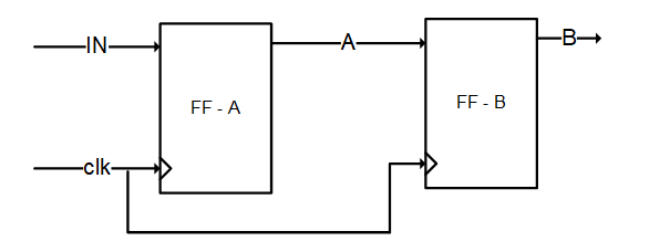
Figure 1: Single Clock domain
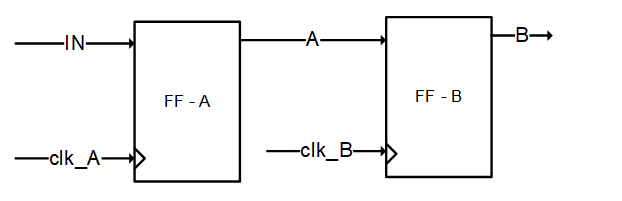
Figure 2: Clock Domain Crossing Path
Another fundamental concept to tackle the multiclock designs is metastability. In layman’s terms, metastability is referred as unstable or intermediate state. When applied into the digital design domain, it means that a FF can enter a state where output might not have reached to its final expected value and can oscillate between 0 or 1. The signal will stabilize after some time but that depends on FF type and the PVT conditions. Metastability cannot be avoided in digital design but can be handled properly by using different Clock Domain Crossing (CDC) techniques (discussed later) so that proper functionality of the design is intact.
For proper operation of the flip flops, the inputs and clocks must satisfy the setup and hold requirements of the FFs. In figure 2 above, the signal A is asynchronous to destination clock domain, since there is no relation between clk_A and clk_B. Once an asynchronous signal is encountered into a clock domain, the setup and hold timings constraints are very unlikely to be met, and thus the FF can enter a metastable state. In picture below the output A of the FF-A changes very close to the pos-edge of the clk_B and thus violates the setup of the FF-B. The output of FF-B will go into metastable state and thus cannot settle to either 1 or 0. This can lead the downstream FFs in the clk_B domain sample wrong value or worse go into metastable state as well.
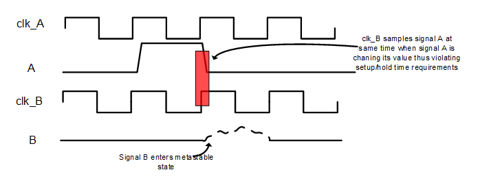
Figure 3: Setup/hold violation leading to metastability
Metastability occurrence of a given FF can be predicted by using a parameter called MTBF (Mean Time Between Failure) and is measured in years. Without going into much of the math, the conclusion is that it is possible to calculate MTBF given that we know the data rate at the input of the FF and the clock frequency of the FF.
Now as we understand metastability and its causes, we can look what are different techniques we can use to handle these situations in digital design.
One of the most common way to handle Clock Domain Crossing (CDC) is usage of synchronizer circuits. Synchronizer circuits purpose is to protect the downstream logic to go into metastable state by minimize the probability of the metastability and increase MTBF. One of the basic synchronizer circuit is a dual flip flop synchronizer (also called 2-FF synchronizer).
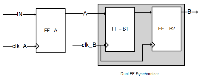
Figure 4: CDC using Dual FF Synchronizer
A dual flip flop synchronizer is a circuit where two Flip Flops are connected back to back in the destination clock domain. If the first flip flop goes into metastable state because of setup/hold violations, the second flip flop give enough time for the first flop to come out of metastable state. The receiving logic will only use the output from second FF. Theoretically it is possible that first FF is still in metastable state when second FF samples the value and thus incorrect value can be sampled which will/can result in malfunction of the design (once in every MTBF years). Dual FF synchronizers are quite good for most of the digital designs however for certain very high speed clock frequencies, the MTBF can be increased more by either using special cells provided in technology libraries or/and using more than 2 stages of the FFs as synchronizers (3 or 4 stages of FFs).
These 2 FF synchronizer circuits work very well for most of the applications that involve single bit control signals and where the input toggle rate is less than the destination clock frequency or in other words, there will be no data loss if destination clock frequency is more than 1.5 times of source clock frequency. However, if the source and destination clock frequency are almost same or destination clock frequency is slow, then source must keep its value stable for destination to capture it, before changing to next value. This can be handled by a handshake Clock Domain Crossing (CDC) technique.
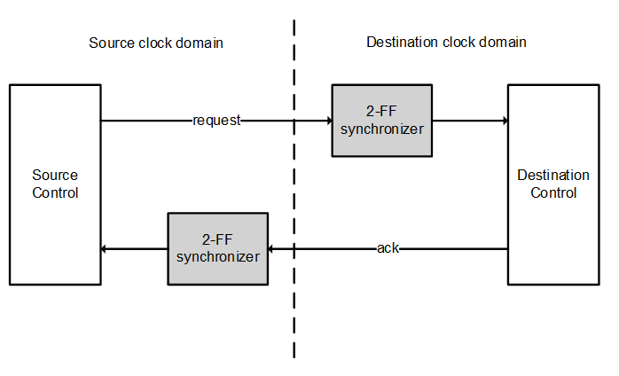
Figure 5: Handshake CDC technique
In handshake technique, the source domain sends the “request” signal to destination domain which uses a 2-FF synchronizer. Once the destination domain receives the request, it sends an “ack” signal to the source domain which uses 2-FF synchronizer to synchronize it. The ack signal indicates to the source that destination has received the value and source can update its value. There are many implementation versions of the handshake mechanism, but the principle remains the same – synchronizing the request and ack signals. The same technique can be applied to do a data bus transfer from source clock domain to destination clock domain. The request will indicate a new value on the bus where as ack will indicate that data bus can be updated.
The above mechanism does have one drawback in terms of bandwidth usage of the interface. For handshaking mechanism, the data bus cannot be updated while receiving the ack signal. For applications where this is a bottleneck, this can be solved by using Dual Clock Asynchronous FIFO. Correctly designed FIFOs can increase bandwidth across the interface while still maintaining reliable communication across channels.
Dual Clock Asynchronous FIFO can be viewed as container of data where sender pushes the data in at source clock rate and receiver pops out the data at destination clock rate. The depth of the FIFO should be enough so that it cannot overflow or underflow the data.
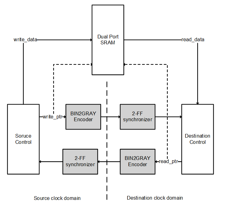
Figure 6: Asynchronous FIFO based CDC
This Clock Domain Crossing (CDC) technique requires a dual port SRAM, a source control block which controls the write pointer (address where the data should be written in SRAM), a destination control block which generates the read pointer (address where the data should be read in SRAM) and binary to gray encoder blocks along with 2-FF synchronizer circuits. The pointers are managed as circular buffer by respective control blocks. However, to know when to write (FIFO not being FULL) and when to read (FIFO not being empty), the source and destination control blocks need to have a view of read and write pointers respectively. Transferring of the pointers to another clock domain is not straight forward. Since pointer is a multibit signal so using a 2-FF synchronizer directly is not an option. For this reason, both pointers are passed through a Binary to Gray Encoding block. This makes sure that values when transferred, only one bit of the vector gets updated from one clock to another clock and thus eliminates the problem of synchronizing multibit bus on a clock edge. An example of 4-bit Gray Encoder is shown below
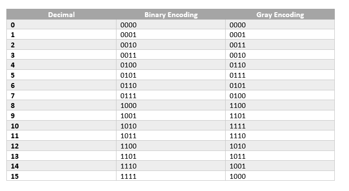
Table 1: Binary and Gray Encoding for 4-bit values
Looking for prices?
Calculate your die per wafer (DPW)
Start your SoC/ASIC design today, click here


