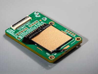
The sensor leverages a spray-coated layer of quantum dots, nanoscale semiconductor crystals tuned to absorb different wavelengths, deposited directly onto standard CMOS chips—the same cost-efficient platform used in smartphones. This direct-conversion design eliminates the need for bulky scintillators, complex hybrid bonding, or expensive materials like InGaAs, unlocking a new class of lightweight and affordable sensors.
Key technical benefits include:
- Direct X-ray detection with high spatial resolution
- Sensitivity across 400–1300 nm, including visible, near-infrared, and SWIR
- Nearly 100% fill factor, preserving pixel density and power efficiency
Enabling safer healthcare, smarter industry
By combining quantum dot photoconversion with mass-producible CMOS technology, this sensor bridges performance and affordability in fields where advanced imaging has been cost-prohibitive:
- Healthcare: Portable X-ray devices and mammography systems with reduced radiation dose
- Industrial inspection: Non-destructive testing of aircraft components and machinery
- Agriculture & recycling: SWIR imaging for crop health monitoring and material sorting (e.g., plastics, fabrics, organics)
“This innovation is a step change for multispectral imaging,” said Nadim Maamari, Group Leader for Edge AI and Vision Systems at CSEM. “It’s a platform that breaks down cost and size barriers, bringing cutting-edge imaging to markets that couldn’t previously afford it.”
Born from aerospace innovation
The sensor was developed under the SWISSMODICS project, led by CSEM and funded by the EU’s Clean Sky 2 program, with additional support from the Swiss State Secretariat for Education, Research, and Innovation (SERI) under the SwissChips initiative. Originally designed for embedding into aircraft structures to detect internal damage without disassembly, the technology now offers wide-spectrum imaging benefits across multiple industries.