From Gate Driver Architecture to Silicon Production
Developing a custom gate driver IC requires specialized expertise in analog and mixed-signal design, high-voltage semiconductor technologies, fast switching circuits, protection functions and power electronics.
Whether your application involves electric vehicles, GaN or SiC power converters, robotics, industrial motor control, renewable energy or AI data centers, a custom gate driver ASIC can improve switching performance, reduce system complexity and integrate multiple functions into a single semiconductor chip.
AnySilicon connects companies with experienced gate driver IC design partners, supporting projects from initial specifications and technology selection through circuit design, tapeout, silicon validation and volume production.
GET 3 GATE DRIVER ASIC DESIGN QUOTESFind qualified semiconductor design companies for your gate driver IC development project.
What Is a Gate Driver IC?
A gate driver IC controls the switching of power semiconductor devices, including silicon MOSFETs, IGBTs, GaN HEMTs and SiC MOSFETs.
Power transistors require appropriate gate voltages and sufficient current to switch efficiently. A gate driver converts low-voltage control signals from a microcontroller, DSP or power controller into suitable gate-drive signals.
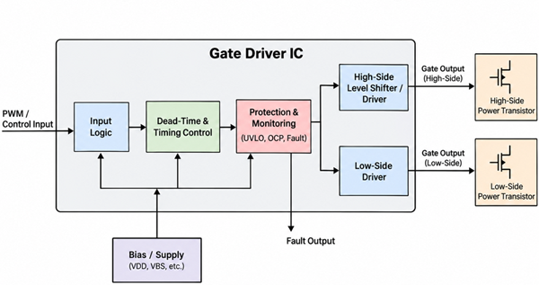
The gate driver is a critical interface between the control circuitry and the power stage.
Typical functions include:
- High-side and low-side gate driving
- Gate-voltage regulation
- Programmable source and sink drive current
- High-voltage level shifting
- Dead-time generation and control
- Undervoltage lockout (UVLO)
- Short-circuit and overcurrent protection
- Desaturation detection
- Active Miller clamping
- Fault reporting and diagnostics
- Safe shutdown and soft turn-off
- Digital configuration and monitoring
Not every gate driver requires all these functions. The appropriate architecture depends on the power transistor, switching topology, bus voltage and application.
Gate Driver ASIC Applications
Custom gate driver ICs are used across multiple power electronics applications.
| Application | Typical Design Requirements |
|---|---|
| Electric vehicle traction inverters | SiC/IGBT driving, isolation, protection |
| Industrial motor drives | High-side/low-side driving, diagnostics |
| AI server power supplies | Fast switching, efficient GaN power stages |
| Robotics | Compact drivers, protection, high integration |
| Solar inverters | High-voltage operation, robustness |
| EV charging systems | SiC gate control, isolation, fault handling |
| Battery energy storage | Power conversion, safe shutdown |
| Industrial DC-DC converters | Switching-speed optimization, precise timing |
| Consumer power supplies | Low cost, small footprint, efficient switching |
For example, a manufacturer developing a 650V GaN power converter may require a custom driver with carefully controlled gate voltage, short propagation delay and high immunity to switching transients.
An automotive supplier developing an 800V traction inverter may instead require an isolated SiC gate driver with advanced fault detection and functional-safety considerations.
Typical Gate Driver ASIC Architecture
A custom gate driver IC may integrate several analog, digital and high-voltage blocks.
Controller / PWM Input → Logic & Protection → Level Shifting / Isolation → Gate Driver Output → External Power Transistor
Additional functions can include:
- Programmable dead-time control
- Bootstrap or floating supply management
- Temperature and voltage monitoring
- Digital configuration registers
- Fault reporting
- Gate-current adjustment
High-side and low-side drivers may be integrated into one IC. Isolation can be implemented on-chip, through specialized isolation technology, or using external components, depending on the electrical and safety requirements.
A major design challenge is maintaining reliable operation under high dV/dt conditions while minimizing propagation delay, switching losses and unwanted transistor turn-on.
GaN vs. SiC vs. Silicon Gate Driver Design
Different power semiconductor technologies require different gate-driver architectures.
| Parameter | Silicon MOSFET / IGBT | GaN HEMT | SiC MOSFET |
|---|---|---|---|
| Gate-drive requirements | Device dependent | Tight voltage control often essential | Higher drive voltage often required |
| Switching speed | Moderate to high | Very high | High |
| Switching transient immunity | Important | Particularly important | Particularly important |
| Negative turn-off bias | Sometimes used | Device dependent | Frequently considered |
| Typical applications | Motor drives, power supplies | Fast converters, data-center power | EV inverters, high-power converters |
| Main design challenge | Efficient, robust switching | Gate-voltage margin, parasitics | Protection, isolation and fast fault response |
GaN devices can support high switching frequencies, but their gate-drive requirements are often more restrictive than those of conventional silicon MOSFETs.
For example, some enhancement-mode GaN devices use approximately 6V gate-drive voltage. The exact requirements depend on the device manufacturer and technology.
SiC MOSFET applications frequently require higher positive gate-drive voltages, sometimes combined with negative turn-off bias to improve switching robustness.
The driver must be designed for the selected transistor rather than assuming that one gate-drive architecture is suitable for all wide-bandgap devices.
Key Gate Driver IC Specifications
Before selecting a design partner, customers should define their electrical and performance requirements.
The following table shows illustrative specifications for a custom high-speed gate driver ASIC.
| Parameter | Example Design Target |
|---|---|
| Power-stage bus voltage | 48V–800V |
| Gate-drive output voltage | Device dependent |
| Peak source current | 2A–10A |
| Peak sink current | 2A–10A |
| Propagation delay | Below 100ns |
| Delay matching | Below 10ns |
| Switching frequency | 100kHz–2MHz |
| Protection | UVLO, OCP, fault reporting |
| CMTI | 100kV/µs or higher, where required |
| Operating temperature | −40°C to +125°C |
| Potential technology | 180nm / 130nm BCD or specialized HV technology |
| Packaging | QFN, SOIC or isolation-compatible package |
All values are illustrative engineering targets, not specifications guaranteed by a particular process or design service. Some combinations may require specialized technology, packaging or external components.
The bus voltage is not necessarily the same as the voltage experienced by the IC’s output driver transistors. Architecture, level shifting, isolation and device ratings determine the actual semiconductor process requirements.
Selecting the Right Semiconductor Process
Gate driver ASICs are frequently developed using high-voltage CMOS, BCD or specialized semiconductor technologies.
BCD (Bipolar-CMOS-DMOS) processes can combine low-voltage control logic, analog circuits and high-voltage transistors on a single chip.
| Technology | Potential Applications |
|---|---|
| 350nm HV CMOS / BCD | High-voltage analog and industrial drivers |
| 180nm BCD | MOSFET drivers, motor drivers, integrated protection |
| 130nm BCD | Compact mixed-signal gate drivers, digital control |
| HV BCD-on-SOI | Applications needing enhanced isolation and robustness |
| Specialized GaN IC technology | Monolithic GaN power-stage and driver integration |
A smaller technology node is not automatically more suitable.
For gate driver ICs, voltage capability, current-driving performance, parasitic capacitance, device isolation and reliability may be more important than transistor density.
Process selection should also consider:
- Available LDMOS and high-voltage devices
- Isolation structures
- Thick-metal options
- ESD protection
- Analog and digital IP availability
- Automotive qualification requirements
- Wafer cost and manufacturing capacity
The exact process capabilities and voltage options must be confirmed with the foundry.
How Much Does Custom Gate Driver IC Design Cost?
Custom gate driver development involves non-recurring engineering (NRE), including architecture, circuit design, simulation, layout, verification and silicon characterization.
Costs depend on the required voltage range, protection complexity, isolation requirements, design reuse and qualification level.
Illustrative Gate Driver ASIC Development Budgets
| Development Scope | Planning Budget (USD) |
|---|---|
| Feasibility study and architecture | $25,000–$100,000 |
| Relatively simple non-isolated gate driver ASIC | $250,000–$700,000 |
| High-voltage driver with integrated protection | $700,000–$1.5 million |
| Complex isolated or automotive gate driver | $1.5 million–$3 million+ |
These are preliminary planning estimates, not published market averages or supplier quotations. Depending on scope, mask sets, fabrication, packaging, production test, third-party IP, qualification and additional silicon revisions may be charged separately.
Prototype Manufacturing Costs
Multiproject Wafer (MPW) programs allow multiple chip designs to share manufacturing resources, potentially reducing prototype fabrication expenses.
As one published example, EUROPRACTICE’s 2026 schedule lists an X-FAB 180nm XH018 CMOS eFlash design with selected optional modules at approximately €16,900 for a 10mm² prototype, under the stated standard-price conditions.
This is an example of prototype fabrication pricing, not a complete gate driver development quotation. Process compatibility, optional high-voltage devices and availability must be confirmed.
Gate Driver ASIC Development Schedule
A custom gate driver IC may require approximately 12–24 months from initial specification to production readiness, depending on complexity, process availability and qualification requirements.
| Development Phase | Indicative Timeline |
|---|---|
| Requirements and feasibility | Months 1–2 |
| Architecture and foundry selection | Months 2–4 |
| Circuit design and simulation | Months 4–8 |
| Layout, verification and signoff | Months 8–11 |
| Tapeout, fabrication and packaging | Months 11–15 |
| Silicon characterization | Months 15–18 |
| Qualification and production preparation | Months 18–24 |
Phases may overlap. Reused IP can shorten development, while additional silicon revisions or qualification requirements may extend it.
Important validation activities include propagation delay, switching behavior, gate-drive strength, dV/dt immunity, protection response time, thermal performance and reliability testing.
For automotive projects, additional activities may include AEC-Q100 qualification and functional-safety analysis where applicable.
When Does a Custom Gate Driver ASIC Make Financial Sense?
A custom ASIC may become attractive when an existing gate driver solution requires too many external components, cannot meet performance requirements or carries excessive recurring cost.
Consider a hypothetical commercial example:
| Parameter | Example |
|---|---|
| Custom development NRE | $600,000 |
| Annual production volume | 300,000 units |
| Product lifetime | 4 years |
| Total production volume | 1.2 million units |
| Recurring system cost saving | $0.70/unit |
| Total saving before NRE | $840,000 |
| Net saving after NRE | $240,000 |
Under these assumptions, development investment is recovered after approximately 857,000 units.
Actual economics depend on wafer cost, yield, packaging, testing, manufacturing volume, inventory and development risks. The cost saving must reflect the complete recurring solution, not simply the packaged ASIC price.
How to Select a Gate Driver IC Design Partner
Choosing an experienced semiconductor design company is critical for high-speed and high-voltage applications.
- Relevant silicon experience: Proven GaN, SiC, MOSFET or IGBT gate driver designs.
- High-voltage design expertise: Experience with level shifting, isolation and BCD processes.
- Protection design: UVLO, desaturation detection, Miller clamping and fault handling.
- Foundry access: Suitable PDKs and relationships with specialty foundries.
- Verification and validation: Experience with switching transients, parasitics and post-silicon characterization.
- Manufacturing support: Capability to manage tapeout, packaging, testing and qualification.
- Commercial arrangements: Defined NRE, milestones, IP ownership and deliverables.
AnySilicon helps customers identify semiconductor design companies with experience relevant to their requirements.
Frequently Asked Questions
Can a custom gate driver ASIC support GaN and SiC devices?
Yes, but the design requirements differ. Gate-drive voltages, switching behavior, protection functions and integration options must be optimized for the selected power transistors.
Can high-side and low-side drivers be integrated into one IC?
Yes. Many gate driver architectures integrate high-side and low-side functions, although the feasibility depends on bus voltage, isolation requirements and the selected semiconductor process.
Is 180nm BCD suitable for a high-voltage gate driver?
Potentially. Mature BCD technologies are widely used for analog and high-voltage circuitry. However, process suitability must be evaluated against the actual device voltage, isolation, current and performance requirements.
Can AnySilicon help with turnkey gate driver development?
AnySilicon connects customers with ASIC design companies offering services that may include architecture, custom circuit design, physical implementation, tapeout, silicon characterization, testing and production support.
Find the Right Gate Driver ASIC Design Partner
Whether you are developing a GaN power converter, SiC inverter, industrial motor controller or automotive high-voltage application, selecting the right design partner is essential.
AnySilicon helps you identify suitable gate driver ASIC design companies based on your technical requirements, budget and development schedule.
Submit your specifications and let AnySilicon help identify up to three relevant partners for your project.
GET 3 GATE DRIVER IC DESIGN QUOTESStart your custom gate driver ASIC development project with AnySilicon.