

What is DDR?
As the name says Double Data Rate, DDR is the class of memory which transfers data on both the rising and falling edge of clock signal to double data rate without increase in frequency of clock. It uses PLLs (Phase Locked Loops) & self-calibration to reach required timing accuracy.
DDR is most critical IP to SoC’s successful operation, because processors in SoC typically spends the majority of its cycles on reading and writing to DDR memory. The self-calibrating logic precisely measures both the latency and phase difference between DDR clock and system clock and aligns the capture of DDR data within the timing window. Timing calibrating logic also maintains performance of DDR memory as temperature and supply voltage fluctuates during system operation.
DDR Implementation Complexities:
Deep submicron SoC (ASIC) designs integrate DDR memory subsystems that operate at multi-GHz clock rates, resulting in read-write timing margins measured in picoseconds. This concerns Designers about static variations due to process and dynamic variations due to system operating conditions such as temperature and voltage.
DDR IP Hardening:
A DDR Memory Interface IP Solution consists of DDR Controller, PHY & Interface. When we refer to the DDR memory subsystem, we are referring to the host System-on-Chip (SoC) controlling and accessing the DDR memory, the interface and interconnect between the host and DDR memory devices, which is typically a PCB, and the DDR SDRAM device itself.
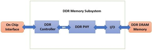
Some key parameters like DDR modes, frequency ratio and memory data width, must be consistent between DDR PHY and DDR Controller.
DDR PHY Blocks Overview
DDR PHY Implementation is divided in internal blocks implementation and TOP implementation. Generally, DDR PHY has five types of blocks as below. Depending on the DDR configuration these block can be changed as per logic.
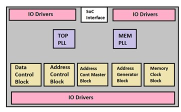
For DDR we have Timing Relation between DQ – DQS and CA – clock signals. For DQ-DQS Relation Read/Write Data Macro blocks are responsible. Whereas control address-clock (CA-clk) Relation is responsible for control-address-command interface connection.
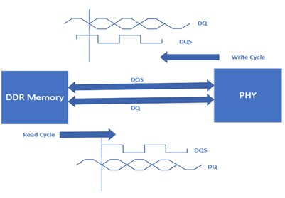
Phase of DQS relative to signal DQ depends on whether it is read or write operation. In Read operation phase, DQS is shifted by 90 degrees with respect to DQ and it will be edge aligned. While in Write operation DQS is central aligned with DQ. As shown in below figure.
Floorplanning Guidelines:
Base of closing DDR is mainly dependent upon Floorplanning. Hence, there are guidelines, which need to be followed during floorplan.
Placement Guidelines:
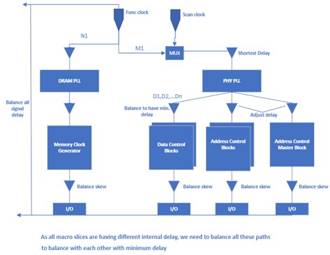
Top Clocks & Skew Balancing Guidelines:
The following are the clock balancing requirements:
MODELLING OF SKEW RELATED STD. CELLs:
In IP there are many hierarchical cells for which the net length should be minimum for those hierarchical cells it is beneficial to make some macro structure which include these cells with the power and signal routing and use it as a macro in the design to minimize the net length. So we can use the extract model from netlist for the same.
Why we model the cells?
Library Cell Delay Variation Impacting Skew:
Balancing Skew/Data paths across multiple corners is tough task as delay variation in cells plays vital role in lower technology node. Meeting same skew value for multiple data bit line which are greater than 2000um long, makes this job even harder. Few cases we will understand which are substantially important before fixing timing issues.
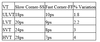
We have seen that across multiple VT, delay variation ratio between ss/ff changes drastically.
Here is example of bufx2:
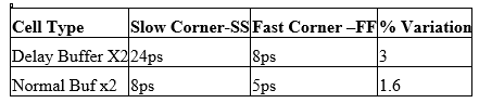
2. Setup-Hold Critical Paths and Delay Buffers
DDR have very complex clock constraint. There are many cases where registers are getting multiple clock in functional mode. Frequency for these Clocks are phase shifted. This causes multiple paths to fail for setup and hold. Such cases can be addressed by balancing clock at Mux point. Next step would be lowering down data paths delay by upsize/Vt swap such that it impacts min delay values for these stages as less as possible. Hold may be still violating but Setup may get fixed by minimal margin. To Address Hold using Delay-Buffer may not be wise decision as delay variation is more between SS & FF.
Here is example of delay-bufx2 & bufx2:
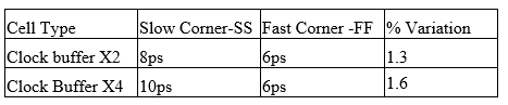
3. CK-Buffer x2-x4 variation across ss/ff
Up sizing CK-Buffers may not be feasible in some cases where skew is very critical. We have observed that delay variation changes across same cells by up sizing or downsizing across SS &FF.
Let’s take example of ck-buf x2 & ck-buf x4:
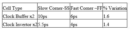
4. CK-Buffer & CK-Inverter variation across ss/ff
We may add clock Buffer to balance skew but as window size is so small that delay variation in SS & FF may fix skew in one corner but degrade in another corner.
Let’s take a look at these variations:
IR & EM Closure:
DDR uses strict skew balancing guidelines so design will have x12 or x16 cells in data and clock path. There will be occurrence of IR & EM violations due to bigger drivers.
EM Fixes need to be done very carefully as minor movement in net routing may affect skew directly. We can prevent such cases by applying double width for such critical nets in PnR.
IR cases can be taken care during PnR by adding two side decap around clock cells and phase generator cells, big drivers.
References:
Authors:
Maulik Patel – Maulik has experience in ASIC implementation for Mobile CPU, Wireless SoC, DDR-IP, Network SoC, Bluetooth. He has done multiple tapeouts for Qualcomm, Broadcom, Cypress, Cadence, and Juniper networks. Maulik is currently working with eInfochips (an Arrow Company) on 16nm ASIC design as Technical Lead-II. His main interests are Low Power Implementation, Clock Tree Synthesis for High-frequency design, and IP Hardening.
Darshan Bhuva – Darshan is working with eInfochips (An Arrow Company) as a Physical Design Engineer for 3 years. He has a brief implementation experience in lower geometry. He has experience in IP Hardening, and Networking ASIC.
Pooja Bhadaniya- Pooja is working with eInfochips (an Arrow Company) in the Physical Design domain having 2.5+ years of experience. She has done multiple tapouts in IP Hardening and Network SoCs.
This post was originally published on DnR.


