Design for Testability (DFT) engineer is an indispensable cornerstone within the semiconductor industry, providing a vital framework that ensures the reliability, efficiency, and cost-effectiveness of integrated circuits. Its primary objective revolves around embedding testability features directly into the design phase of these intricate circuits, thereby facilitating streamlined testing procedures, early fault detection, and expedited fault diagnosis during manufacturing. By incorporating DFT principles, engineers significantly mitigate risks associated with defects, accelerate time-to-market, and uphold stringent quality standards, thus fortifying the foundation upon which the semiconductor industry continues to innovate and thrive.
In this article we will discuss the role of design for test engineers, their responsivities, workflow, tools and more.
Key Role and Responsibilities for DfT Engineers
Design for Testability (DFT) engineers play a crucial role in ensuring the effectiveness and reliability of semiconductor chips. Their key responsibilities include:
- Test Structure Integration: DFT engineers work on integrating specific test structures and logic directly into the chip’s architecture. This integration involves strategically placing components within the design that allow for comprehensive testing. They create and embed features such as scan chains, Built-In Self-Test (BIST) modules, and other test access mechanisms that enable thorough testing of the chip’s functionality.
- Test Methodologies Development: These engineers are responsible for developing innovative and efficient test methodologies. They design algorithms and strategies aimed at detecting potential faults or defects within semiconductor devices. This involves creating complex testing scenarios and protocols to thoroughly evaluate different functionalities and potential failure points of the chip.
- Compliance with Standards: DFT engineers ensure that the testability features implemented in semiconductor designs comply with industry standards and protocols. They stay updated with the latest standards and guidelines to ensure compatibility across diverse manufacturing and testing platforms. By adhering to these standards, they enable easier interoperability and compatibility between different chips and testing equipment.
DFT for ASIL standards involves implementing robust testing mechanisms within the design phase to ensure the functional safety of automotive electronics.
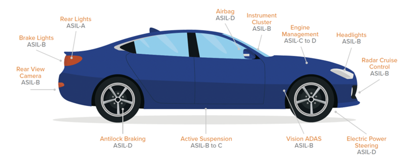
Figure 1: Automotive Safety Integrity Level (ASIL) Standards
- Collaboration with Design Teams: Additionally, DFT engineers collaborate closely with various teams, including design, verification, and manufacturing, to ensure that the testability features are seamlessly integrated into the chip design without compromising its performance or functionality. Their work significantly contributes to the overall quality, reliability, and manufacturability of semiconductor products in the market.
- Debugging and Troubleshooting: In the event of test failures or issues during manufacturing, DFT engineers troubleshoot problems, analyse test results, and identify the root causes of failures. They work on solutions to rectify these issues and ensure the integrity of the circuits.
Skills and Qualifications for DfT Engineers
A typical DFT engineer typically holds a degree in Electrical Engineering, Electronics Engineering, or a related field. Key skills required for this role include:
- Proficiency in digital design and verification methodologiesA DFT engineer demonstrates an adept command of digital design principles, navigating the intricacies of RTL coding and simulation. This proficiency enables the conceptualization and implementation of intricate circuit designs while rigorously verifying their functionality and performance at the Register Transfer Level.
- In-depth knowledge of DFT architectures and methodologies: Beyond basic comprehension, a DFT engineer delves deeply into the nuances of DFT architectures. Their expertise spans across pivotal methodologies like scan chains, Built-In Self-Test (BIST), and the intricate intricacies of Design for Debug (DFD).
- Familiarity with Automatic Test Pattern Generation (ATPG) tools and fault models to generate efficient test patterns for manufacturing tests.
- Expertise in scripting languages (e.g., Perl, Python). These languages serve as invaluable tools for automating testing procedures and conducting comprehensive data analysis, streamlining the testing phase and enhancing overall efficiency.
- Strong understanding of industry-standard test protocols and standards (e.g., IEEE 1149.1, IEEE 1500).
In short, a solid education and a wide range of skills in tech, tools, and industry rules are key for a skilled DFT engineer. They’re vital for handling the complexities of modern semiconductor design and manufacturing.
Workflow of a DFT Engineer
The role of a DFT engineer involves a structured workflow aimed at seamlessly integrating crucial testability elements into chip designs, ensuring the reliability and efficiency of the final product. This workflow encompasses several key phases, each playing a pivotal role in guaranteeing the integrity of the integrated circuits:
- Test Architecture Definition: At the onset, the DFT engineer engages in defining the blueprint for test structures and strategies. They meticulously tailor these structures based on the specific design requirements while selecting appropriate DFT methodologies. This phase sets the foundation for robust testing protocols aligned with the circuit’s intricacies.
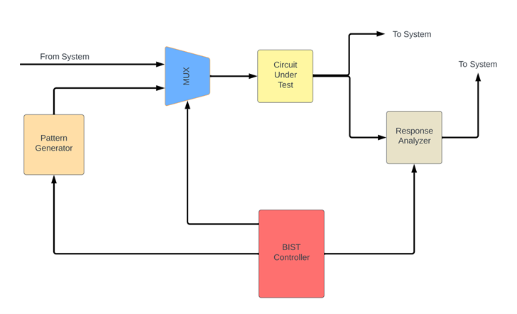
Figure 2: Typical BIST Architecture
- Test Pattern Generation: Leveraging cutting-edge ATPG tools, the engineer crafts intricate yet efficient test patterns. These patterns are meticulously designed to achieve high coverage, adept at uncovering faults and defects lurking within the complex circuitry. The emphasis here lies on generating optimized patterns crucial for comprehensive testing.
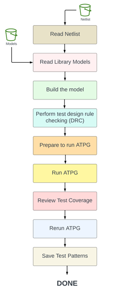
Figure 3: ATPG Workflow
- Design Verification and Simulation: This phase entails a rigorous cycle of simulations and verifications. The DFT engineer meticulously examines and scrutinizes the effectiveness of the integrated test structures and methodologies. Through thorough simulations, they ensure that the implemented testability features seamlessly align with the design’s intricacies, striving for optimal performance.
- Post-Silicon Validation: Collaboration takes centre stage as the DFT engineer works closely with validation teams in the post-silicon phase. Together, they conduct extensive validation exercises, meticulously verifying the functionality and efficacy of the integrated testability features. This collaborative effort aims to validate the chip’s performance in real-world scenarios, ensuring its reliability and adherence to expected standards beyond the design phase.
In essence, the workflow of a DFT engineer is a meticulously orchestrated process, spanning from the foundational architectural planning to the collaborative validation phase. Each stage is instrumental in fortifying the integrity and reliability of integrated circuits, emphasizing seamless integration, efficiency, and rigorous testing protocols.
Tools and Software (Design for Test)
DFT engineers rely on specialized tools and software to carry out their tasks efficiently. They commonly use various tools in the DFT domain:
- ATPG tools: Examples include Synopsys TetraMAX and Mentor Graphics Tessent.
- Simulation and verification tools: These encompass Cadence Incisive and Mentor Graphics ModelSim.
- Scan synthesis tools: Some of the prominent tools in this category are Cadence Encounter Test and Synopsys DFTMAX.
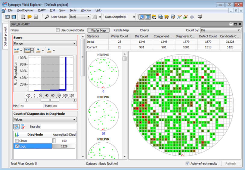
Figure 4: EDA Tools play a crucial role in DFT Engineering
Challenges in DFT Engineering
DFT (Design for Testability) engineers are tasked with ensuring that complex electronic designs can be effectively and efficiently tested during manufacturing. While this field is essential for identifying and resolving issues before products reach the market, DFT engineers face several challenges:
- Timing Closure and Testability: Addressing timing closure issues while integrating testability features can be challenging. Ensuring that test structures do not adversely affect the chip’s timing performance is crucial. Balancing the timing requirements of the design with the insertion of test features without compromising speed or functionality is a critical task.
- Design for Manufacturability: DFT engineers must consider manufacturing variations and process defects while designing test structures. They need to create robust test mechanisms that are resilient to these variations and can effectively detect faults in chips across different manufacturing lots and process nodes.
- Scan Chain Length and Compression: As chip sizes increase, managing scan chain lengths becomes more complex. Longer scan chains can increase test application time and area overhead. DFT engineers work on implementing compression techniques to reduce the number of test patterns and minimize the length of scan chains without compromising fault coverage.
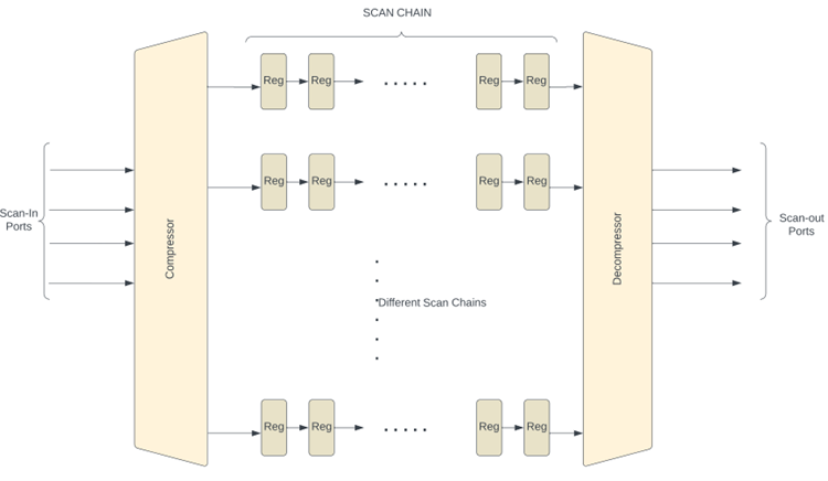
Figure 5: Compression/Decompression (CODEC) Logic helps manage the number of scan chains
- Post-Silicon Validation and Debugging: Validating chip functionality after manufacturing and diagnosing issues in the post-silicon phase is a significant challenge. DFT engineers develop methodologies and tools for efficient post-silicon validation to ensure the chip functions correctly under real-world conditions.
- Security and Test Access: With growing concerns about hardware security, ensuring that testability features do not create vulnerabilities or unauthorized access points becomes crucial. DFT engineers must design secure mechanisms to prevent unauthorized access to sensitive data or functionalities during testing.
- Adapting to Emerging Technologies: Keeping up with advancements in semiconductor technology, such as new architectures, materials, and manufacturing processes, presents a challenge. DFT engineers need to adapt their methodologies and techniques to ensure effective testing and fault coverage in these evolving landscapes.
Overcoming these challenges requires a combination of innovative thinking, in-depth understanding of chip design principles, collaboration across various engineering disciplines, and the continual evolution of testing methodologies to match the complexity and advancements in semiconductor technology.
Trends and Innovations in DFT Engineering
Here are three noteworthy trends and innovations in the realm of DFT engineering:
- Advanced DFT architectures: Development of novel DFT architectures and methodologies to address testability challenges in advanced process nodes, such as 3nm and below.
- AI and Machine Learning in Test Pattern Generation: Utilizing AI-based algorithms to optimize test pattern generation and fault coverage, improving efficiency and accuracy.
- Design for Reliability (DFR): Integrating DFT methodologies aimed at enhancing chip reliability and resilience against aging, wear-out, and environmental factors.
These trends underscore the evolving landscape of DFT engineering, emphasizing the need for innovative solutions to address emerging challenges and drive the development of robust and testable semiconductor devices.
Career Opportunities and Job Outlook
The job market for DFT engineers is robust, driven by the increasing demand for semiconductor products across various industries. Opportunities for DFT engineers exist in:
- Semiconductor Companies: Major semiconductor companies seek skilled DFT engineers to work on cutting-edge chip designs.
- Electronic Design Automation (EDA) Companies: EDA companies develop software tools used in the design and verification of ICs and hire engineers to work on tool development, optimization, and support.
- Startups and Small Firms: Emerging companies focusing on specialized chips, AI hardware, IoT devices, and niche technologies often look for DFT engineers to create innovative chip designs.
- Research and Development: Opportunities exist in research institutions and academia for those interested in pushing the boundaries of chip design through innovative research.
- Consulting and Services: Some engineers work as consultants, providing expertise to multiple companies or offering specialized services in chip design.
Continuous learning and staying updated with the latest advancements in semiconductor technology, tools, and methodologies are essential for career growth in this field. Specializations in areas like advanced process nodes, low-power design, or specific applications (such as AI chips or IoT devices) can also open doors to specialized roles and higher demand in the job market. Additionally, networking within industry forums, attending conferences, and pursuing certifications can enhance professional visibility and create avenues for career advancement in the dynamic field of Design for Testability (DFT) engineering.
In conclusion, DFT engineers play a vital role in the success of semiconductor technology. Their job involves embedding test features into chip designs and collaborating with various teams. They ensure chips work reliably and efficiently by creating smart testing strategies and fixing any issues. With their expertise and dedication, they are essential in driving innovation and ensuring high-quality semiconductor products. They are the unsung heroes shaping the future of technology.


