Dr. Morris Chang is not my hero. He might be the most important person in the semiconductor industry in our lifetime, but he is not my hero. I have nothing against him. I’ve never met him and probably will never will. Instead, I meet my heroes usually after tape-out, when my chip doesn’t function as expected, and nobody can tell me why.
Sounds familiar?
Yes, I am talking about Failure Analysis engineers, who are my real heroes.
To me failure analysis has always been a bit magical. Basically it involves a process of animating and analyzing a chip to determine the root cause of a failure. A skilled failure analysis engineer can take a faulty chip, decapsulate and analyze it, isolate the failure, and pinpoint the reason for a semiconductor device failure. Then he or she can encapsulate it back into its package and hand over the chip back to you, so you can continue with your debug activities. To me, this is semiconductor’s magic at its best.
Failure analysis engineers can encounter a wide array of problems from assembly issues, silicon issues and sometimes design issues. Therefore, he or she needs to master multiple techniques and equipment types to analyze a device and recommend a correction or an improvement.
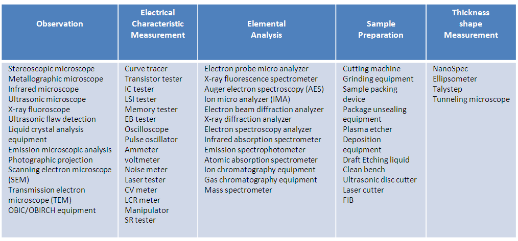
Besides the deep understanding in semiconductor technologies and packaging materials, a failure analysis engineer needs to operate a unique set of equipment and tools, often in concert. Roughly speaking, tolls can be divided into 5 different groups:
It is unlikely to find find the entire set of equipment available in a single lab. Rather, independent labs can typically afford only a few tools.
The following table shows a list of specific equipment for each of these categories.
Surprisingly enough, turnaround time for most failure analysis jobs is relatively short. Provided your FIB instruction are clear and accurate, an average FIB work would not take more a single day, and re-packaging a die back into a QFN package can take up to one hour. Using a failure analysis lab, therefore, is a big time saver compared to the alternative of changing a mask layer or making a new mask-set.
How does failure analysis handle new semiconductor processes introduced by foundries every 2 years? Today’s new breakthrough technology in 20nm and below is FinFET transistors. While ASIC engineers and SoC architects are evaluating how to harness and benefit from such complex processes, the failure analysis folks are wondering if they can cope with such small structures.
We will dive deeper and elaborate on specific failure analysis tools and methods in future posts. In the meantime, please add any comments you may have.
Of course, you’re also welcome to search our directory for vendors providing IC failure analysis services.