

FDSOI stands for Fully Depleted Silicon on Insulator. FDSOI is a planar process technology that provides an alternative solution to overcome some of the limitations of bulk CMOS technology at reduced silicon geometries and smaller nodes.
The FDSOI process has two distinct features. First starting with the substrate, an ultra-thin buried oxide layer is placed on the top of the base silicon. Second, a very thin silicon layer on top, creates the transistor channel. The FDSOI transistor is built above the buried-oxide layer. It has a raised source and drain and a very thin uniform channel under the gate. As the transistor channel layer is very thin, no channel doping is required, which makes the transistor fully depleted. The resulting FDSOI device is shown in the illustration in Fig. 1.1.
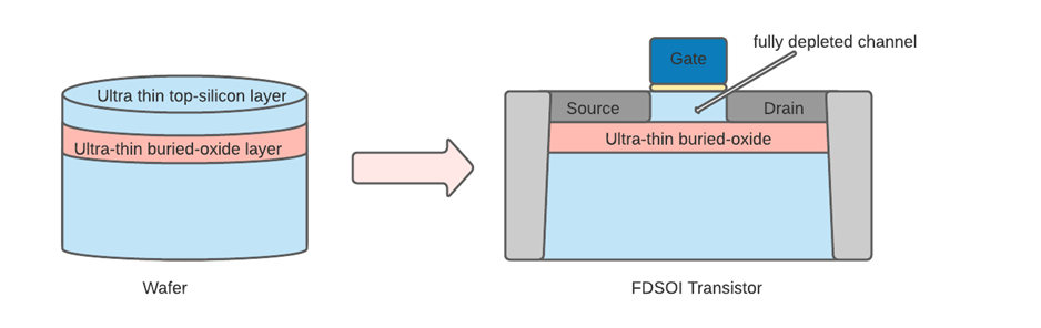
Fig. 1.1: FDSOI transistor
FDSOI is not only an alternative to continued CMOS scaling beyond 28nm node but also proves to be useful in improving the performances of older technology nodes when redeveloped using this process.
The structure of FDSOI devices provides for many striking characteristics that give this technology unique advantages that can be exploited to improve chip design. This article summarizes the characteristics and various elements of FDSOI technology as well as the advances and implementation of FDSOI in the several application fields.
The semiconductor industry today has grown from a niche market into a multiple billion dollar business after the first invention of transistors in 1947. Over the past decades, demands of consumers for more efficient, superior, cheaper and faster devices have fueled the innovation and scaling in CMOS technology and transistor feature size is continuously decreasing. But with each new leading-edge process node, the increasingly dense layout of billions of transistors in a chip is giving rise to issues that degrade the power and performance. For the smaller nodes, cost per transistor is going up. It is becoming increasingly difficult to continue Moore’s Law with each node.
The regular bulk planar transistors have issues in scaling because the channel area underneath the gate is too deep and too much of the channel is too far away from the gate to be well-controlled. The leakage power is going up so much with each smaller node. The channel needs to be well controlled by the gate. One solution for this is the FinFET in which Instead of having a planar transistor with the channel in the silicon wafer itself, the channel is created as a thin vertical fin wrapped by the gate around three sides of the fin. Because the fin is thin and wrapped from all sides so the whole channel is well controlled by the gate. But this is a 3D process and it adds a lot of complexity to the manufacturing. Another more simpler way to do this is using the FDSOI process. Using the insulator layer beneath the thin layer of channel on top helps in greatly reducing the leakage to the substrate. As the channel is ultra thin, the same as in the FinFET case, it is well-controlled by the gate.
The concept of FDSOI devices was first introduced in the early 2000s. In the development of the initial FDSOI devices Leti played a very important role. Soitec was instrumental in developing the FDSOI substrate. The FDSOI ecosystems began to accelerate after the manufacturing process was well developed. Two IDMs, STMicroelectronics and Renesas, also have their own FDSOI technology. STMicroelectronics adopted FD-SOI technology in 2012 and started several projects. STMicroelectronics is now using this technology for many diversified market applications. Renesas has a 65nm version of FDSOI called silicon-on-thin-BOx (SOTB), which targets ultra-low-power MCU markets. A partnership on FDSOI fabrication between ST and Samsung Foundry was announced in 2014. Today, two out of the world’s top foundries offer FDSOI technology fabrication. Samsung offers its 28nm and GF has its 22nm node fully developed for production. Many companies such as NXP, Sony, Mobileye started projects on FDSOI technology after the foundry system was in place. Today the IPs are well developed to make any sort of application possible. Both Samsung and GLOBALFOUNDRIES are also developing its 18nm and 12nm nodes for future production, respectively. In Feb 2017, GF announced its plans to expand the capacity of its Fab 1 facility in Dresden due to market’s growing interest. In September 2017, Soitec announced to re-open its Singapore fab to meet increasing customer demand for wafers.
Over its 20-year history and promising benefits, FDSOI technology has been growing slow and steadily. In earlier years, the growth of FDSOI technology into the mainstream market has been impacted by several factors. The biggest one of them has been the availability, cost, and quality of SOI materials. The SOI wafers should have a thin, uniform, defect-free silicon layer with a high quality of buried oxide. Earlier the supply of these wafers was a limiting and costly factor, but with the emergence of several companies that specialize in offering high quality wafers this is becoming less of an issue. Another issue for FDSOI has been the circuit design, which requires a better understanding of the underlying device physics and processes, otherwise the benefits of high body bias capability might not be fully utilized. Today FDSOI is an emerging technology with a high future potential.
In a CMOS transistor, flow of electrons between gate and source is controlled by the gate. When an appropriate voltage is applied to the gate terminal, it forms a conductive channel beneath the gate and electrons flow between source and drain. When gate voltage is removed, the electron flow is turned off. So the transistor essentially acts as a switch. As the transistor geometries keep shrinking , the length of the gate is also reducing. The gate control over the channel region is also reduced which results in degraded transistor performance such as, there is some leakage current even when the transistor is turned off. This leakage current has been increasing with each smaller node and contributes to a considerable proportion of power consumption. So how can we Improve the control of the gate over the channel in lower technology nodes to improve the transistor performance?
FDSOI technology offers a solution to this problem. In FDSOI a thin layer of insulator called the buried oxide is added to the wafer. On top of this a very thin silicon layer is added to form the channel. To get good performance of the device, a general rule of thumb is that the channel thickness should be around 1/4 of the gate length. As the channel is very thin, it eliminates the need to add dopants to the channel thus making it fully depleted. Due to the buried oxide layer combined with the thin body channel layer, this technology is also termed as ultra-thin body and buried oxide or UTBB.
Let’s take a look at how FDSOI improves performance of the transistor. FDSOI architecture enables CMOS scaling without relying on channel doping. In bulk CMOS transistors dopants are injected into the channel during manufacturing. Different quantities of these dopants leads to random dopant fluctuations which is a major cause of process variation in the transistors. The FDSOI transistor channel is typically undoped which eliminates the random dopant fluctuations while achieving better short-channel control. The process variations are greatly reduced in FDSOI transistors and it offers a superior matching in transistor characteristics. Because of less variation, the margins for process variability can be reduced which can achieve faster performance.
FDSOI transistors improve upon various short channel effects seen in bulk CMOS architectures. In bulk-CMOS transistors, the parasitics between drain and source and the substrate leads to various short-channel effects such as gate-induced drain leakage current, drain-induced barrier lowering and variability in threshold voltage. In FDSOI, the buried layer oxide provides shielding for the source and drain, which reduces these parasitic capacitance.
FDSOI transistor has a shorter effective channel compared to a bulk silicon CMOS on the same technology node. The shorter channel reduces the time period for the electron flow from the source to the drain leading to a faster transistor. FDSOI transistors have a steeper subthreshold slope (SS) as shown in Fig. 1.2, hence the transistor turns on faster (into overdrive), reducing the threshold voltage. This means that same performance can be achieved at a lower supply voltage as compared to the conventional transistor. In bulk CMOS, the sub-threshold leakage current is a major problem at lower technology nodes. Even when the transistor is in standby mode, the leakage current still flows. The buried-oxide layer helps confine the electrons while flowing from source to the drain drastically reducing leakage currents from the channel to the substrate.
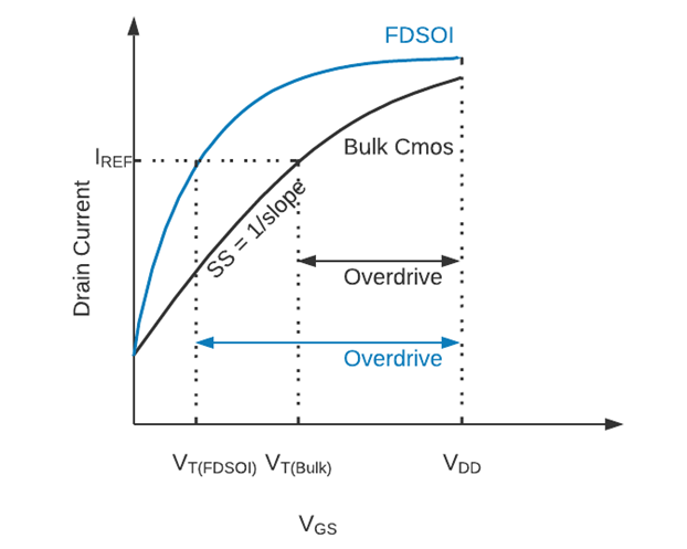
Fig. 1.2: Subthreshold slope in FDSOI
In bulk CMOS, in order to improve transistor performance, a voltage can be applied to the substrate to improve the transistor performance. The forward body biasing of substrate lowers the Vth and facilitates the creation of the channel between the source and the drain resulting in faster switching of the transistor. Similarly a reverse body bias on the substrate increases the effective Vth of the transistor which helps in reducing leakage power consumption. However, In bulk technology, the ability to do body biasing is very limited due to parasitic current leakage and short-channel effects. In FDSOI, the biasing creates a buried gate below the channel due to the presence of the buried-oxide insulator layer. The transistor acts like a vertical double gate transistor. The buried gate on the FDSOI transistor prevents any leakage in the substrate. This allows a much higher range of voltage on the body leading to a significant boost in the performance. The characteristics of the FDSOI vertical double gate transistor allows for much more flexibility in the design. Different voltages can be applied independently to the top and the buried gate which effectively change the characteristics of the transistor from those of a very high performance transistor to those of a very low power transistor.
For better performance in bulk CMOS at lower nodes, a lot of complexities are added in the manufacturing process. The other alternative, FinFet which is a 3D technology, is quite complex and different from bulk-CMOS manufacturing. However, The planar process of FDSOI allows for a simple manufacturing process. It reuses most of the process steps used in 28nm bulk and the overall manufacturing process is less complex leading to lower cycle time and reduced manufacturing costs. FDSOI also makes design reuse much easier as compared to FinFet. When designing a chip in FDSOI, most of the IP blocks can be directly reused from bulk design. Only a few analog parts need to be adapted to FDSOI. FDSOI is a scalable technology, It ensures continuity with planer process and design while improving performance & lowering power consumption.
Answer a few questions and get a recommended shortlist of foundries. Full scoring and a longer shortlist by email.
FDSOI technology has a lot of major benefits for smaller technology nodes. Key benefits of this process are summarized below.
FDSOI devices have a fully depleted channel. In these devices the threshold voltage depends upon polarity of the well and the body bias. For the change in Vt the device doesn’t have to be doped. This reduces the random dopant fluctuations in devices to a great extent. Random dopant fluctuations is a major reason for device match. FDSOI technology offers the lowest device mismatch.
The dynamic power in a design scales with Vdd², So lowering the supply voltage results in lowering the dynamic power consumption. But the device variation in CMOS technology makes it difficult to lower the supply voltage beyond a certain range. But FDSOI can achieve very low supply voltages due to the body bias and its intrinsic low-variability characteristics. FDSOI ability to use a much lower supply voltage presents a unique advantage in applications in which power is a greater challenge than performance.
Full back biasing is a very unique feature in FDSOI technology. This makes it possible to completely tune the threshold voltage through the back gate. Different Vt (Low, mid-range and high) can be simply achieved by using appropriate bias voltages. All the complex Vth adjustment techniques through channel doping can be avoided. Most importantly, it can also be used dynamically. This means that based on the requirement, the same functional block can operate in high or low power mode.
When high-energy particles can interact with silicon, they can generate a significant amount of charges which can flip the memory or transistor logic state. This leads to an increase in the soft errors rate (SER). In FDSOI, devices are completely isolated from the substrate due to the buried oxide layer, so any charge generated in the substrate is unlikely to modify the device logic state. Hence it is less sensitive to SER. This is a very important requirement for safety-critical devices such as automatic car systems.
Latch is a phenomenon in CMOS technology where various parasitic elements of the device forms a low resistance path between power supply and ground which can lead to device high currents and damage to the device .As all the wells in FDSOI technology are isolated by the oxide layer, the latch-up issues of bulk-cmos technology do not appear in FDSOI devices.
For analog designs, meeting the noise, power, leakage and variability requirements is becoming very challenging due to degradation in transistor characteristics as technology shrinks. As FDSOI transistors have improved device matching, gain and parasitics, it can greatly simplify the analog design. The back bias capability in FDSOI also has a lot of potential in designing analog circuits. FDSOI has very high Ft, Ft/FMax, high mmWave self gain which is important for RF blocks. These key characteristics help in superior RF and analog designs.
Below the 28 nm node, new technologies add greater complexity to the manufacturing process. As the nodes keep getting smaller, the more masks are needed to manufacture the chips. This results in increased manufacturing costs as well complex design flow, design verification and more. On the other hand, FDSOI has a simple manufacturing process. It follows most of the traditional bulk-CMOS fabrication process steps with very few changes. FDSOI offers higher performance with reduced manufacturing complexity.
Due to the several advantages of FDSOI such as better control of random mismatch, minimized junction leakage and capacitances, enhanced electrostatic characteristics and simpler manufacturing, this technology offers the best power, performance, area and cost tradeoff among all planar technologies.
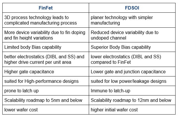
Both FDSOI and bulk-CMOS are planar technologies. Being a planer technology they both have the advantage of having a simpler manufacturing process. Below table lists down some of the key aspects of both technologies.
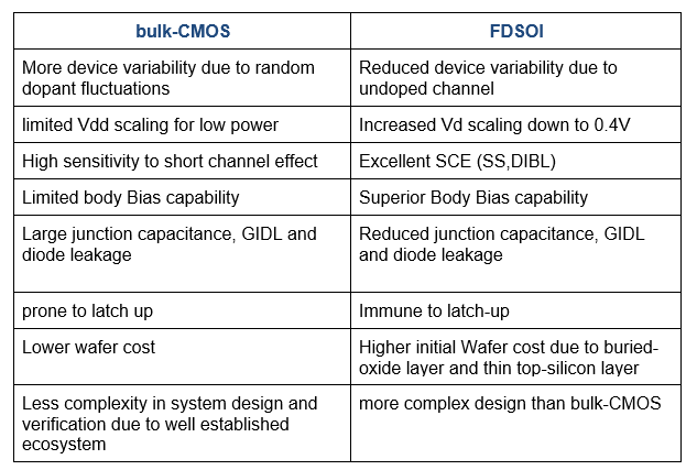
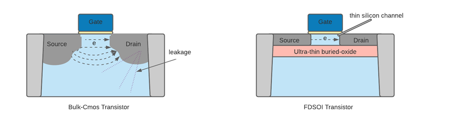
Fig. 1.3: Bulk-CMOS vs FDSOI device
Both FDSOI and Tri-Gate FinFET provide an alternative for bulk-CMOS technology at smaller nodes. They both have a fully depleted transistor where the voltage applied to the gate has a much improved control of the gate over the channel. As a result, the short channel effects are reduced and the power supply can be scaled further down. The lower supply and threshold voltage also leads to lower dynamic power dissipation. FDSOI remains a planar technology, which makes manufacturing much simpler compared to the FinFET devices.
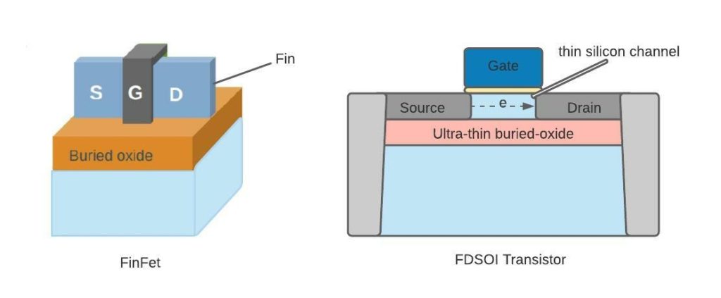
Fig. 1.4: FinFet vs FDSOI device
The below table provides a comparison of the physical and electrical characteristics of both technologies.
Body Biasing is a technique in which voltage can be applied to the substrate to improve the transistor characteristics. Body biasing is perhaps the most interesting feature in FDSOI process technology. Low-Vt, mid-range and high-Vt in a transistor can be achieved simply through back-gate biasing. This body biasing can also be modified dynamically depending on the operating characteristics required at the time.
Due to parasitic currents, the ability to implement body biasing is limited in bulk technology, but the buried gate in FDSOI limits the leakage in the substrate. Thus, it allows a much higher range of the voltage that can be applied to the body which leads to a significant boost in performance. The range of back-gate biasing in FDSOI is increased by a factor of ~10 as compared to the bulk technology.
Due to the presence of an ultra-thin oxide layer in FDSOI, the biasing creates a buried gate below the channel making the transistor act as a double vertical gate transistor. This vertical double gate characteristic allows different voltages can be applied independently at the top and at the buried gate which in turn changes the characteristics of the transistor. The transistor characteristics can transform from high performance to low power transistor by choosing an optimum voltage combination at the buried gate and top gate.
Body bias can be applied either statically or dynamically using the Back Plane through the wells.
There are two ways to apply body bias:
For an NMOS, If VBB is positive, then it is a forward body bias. But, VBB is negative, then it is reverse body bias. Vice-versa is applicable for the PMOS transistors. The types of device structures offered in FDSOI technology are either optimized for RBB or FBB.
The Forward body bias is used to lower the Vth of the device so that the transistor can be switched faster. The low Vth device can achieve high Iᴏɴ current. A higher Iᴏɴ can charge the output capacitance of the transistor faster thus resulting in higher circuit speed. However, the drawback here is that if the Vth is reduced then the leakage current will increase. So there has to be a compromise between speed and power based on design requirements.
The fbb device uses flipped well design as shown in Fig. 1.5. In this design, we have nmos on top of nwell & pmos on top of pwell. The bias voltage is applied on the substrate to lower the threshold voltage of the device. In general, LVT/ULVT devices are optimized for FBB.
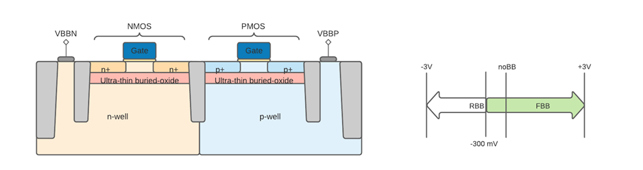
Fig. 1.5: Flip Well FDSOI design
The forward and reverse bias range of the device also depends on the doping of the well in which the transistor is fabricated. Increasing the bias beyond the optimum range creates a parasitic diode between the n+ and p+ wells. For the devices optimized for forward body bias using the flip well design, the effective gate voltage of the transistor can be increased by as much as 3V, but the reverse bias will be limited to -300mV.
Reverse body-biasing (RBB) can be applied to improve the stand-by mode leakage. RBB devices have the traditional CMOS structure as shown in Fig. Here the nmos is on pwell & pmos is on nwell. RBB is applied on the substrate to raise the threshold voltage of the device. RVT/HVT devices in an FDSOI technology are optimized for RBB.
In the devices optimized for RBB, reverse body bias can be extended to -3V, but the forward bias will be limited to 300 mV. However, if only a single transistor is used, NMOS or PMOS transistor (not CMOS), the body bias voltage can be used from -3V to 3V.
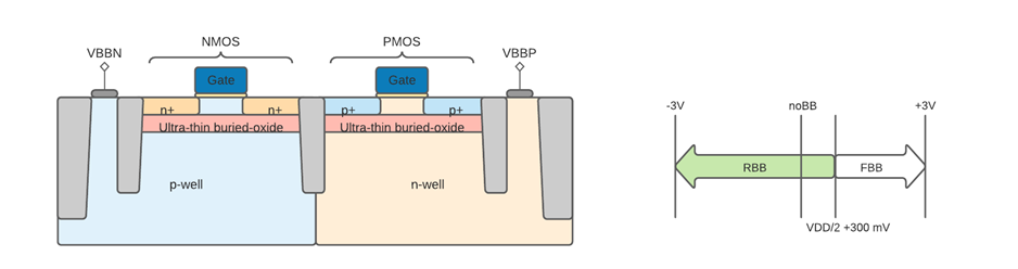
Fig. 1.6: Conventional Well FDSOI design
Body bias is an extremely powerful technique to optimize performance and power consumption. It brings a great flexibility to the designers. There is a tradeoff between leakage & performance of the two types of the devices. Based on the need of the design, if the transistors are going to work in standby mode most of the time RBB can be chosen to reduce the standby leakage. If the design is in the high performance mode most of the time, FBB can be utilized to increase the performance of the design. Body biasing can be used in multiple scenarios such as selective body bias for critical path improvements or for process variation compensation and reliability drift compensation.
While the body bias can be used stand-alone to vary the maximum frequency or power savings, but combining it with different voltage frequency scaling (DVFS) can provide the best performance vs power tradeoffs in the design.
Different characteristics of FDSOI process technology can be utilized for various different applications.
FDSOI is highly suitable for the automotive market due to its reliability and good SER. In the automotive industry, reliable operation is of utmost importance to avoid any catastrophic consequences especially in adverse environments. It can provide a low power and highly reliable solution for ADAS and infotainment systems.
For mobile technology, FDSOI provides a great power-performance-cost tradeoff. It can provide optimized SoC integration solutions for application processors, basebands and transceivers with low power consumption. Due to good analog/RF characteristics it is a great technology for 5G and Radar applications.
FDSOI has a great scope in the IoT market. Different IoT applications such as consumer media, medical, wearable devices, smart home systems, edge computing, require a mix of low power, superior RF and analog performance and low cost solutions. FDSOI can provide the right power and performance balance for these devices at a much lower cost. Its ultra low voltage operation combined with reverse body bias reduces power consumption drastically and enables a huge gain in battery life.
FDSOI technology brings various advantages to networking infrastructure, machine learning, and consumer multimedia applications.
Nowadays customers are demanding more and more design capability with very low power consumption. The FDSOI process has the capability for providing solutions to high energy efficiency designs. It provides improved speed and reduced power consumption through a simple manufacturing process, so the power-performance-area-cost tradeoff is very good as compared to both bulk-CMOS and FinFet. The other thing that is kind of unique to FDSOI is the fact that body biasing can be reused again which is not something that can be done in a FinFet process. Body biasing is simply not effective from 40nm below in terms of a bulk-CMOS planer process as well. So it can actually provide different power options for the design and will deliver in terms of the promise for low power.
Developing and designing any product in a new technology requires the support of an entire ecosystem. The choice of process technology node, foundry or availability of IPs is of critical concern to build these products. Developing any new process technology requires a lot of time and investment from the industry to finally be able to provide cost-effective solutions to the consumer. FDSOI is gaining a lot of interest over the years from major companies in semiconductor industries due to its unique characteristics and will likely to grow more in future. This technology is already supported by multiple foundries and IP solution providers for 28nm & 22 nm. The future roadmap 12nm is already in place and the process can be scaled down below 10 nm as well. In future, FDSOI will continue to provide a cost and power effective solution to diversified markets with this entire support system in place.
Q: What is FDSOI technology?
A: FDSOI (Fully Depleted Silicon-On-Insulator) is a type of semiconductor technology that uses a thin layer of silicon on an insulating substrate to create transistors. It allows for higher performance and lower power consumption than traditional bulk CMOS (Complementary Metal-Oxide-Semiconductor) technology.
Q: What are the advantages of FDSOI technology?
A: Some of the advantages of FDSOI technology include:
Low power consumption: FDSOI transistors can operate at very low voltages, leading to lower power consumption and better battery life for devices that use them.
High performance: FDSOI transistors can switch on and off faster than bulk CMOS transistors, leading to faster devices.
Improved reliability: FDSOI transistors are less prone to reliability issues such as hot carrier degradation and latch-up.
Lower cost: FDSOI technology can be implemented using a simpler manufacturing process compared to other advanced technologies such as FinFETs.
Q: Who is using FDSOI technology?
A: FDSOI technology is used by a variety of companies and organizations in a range of applications, including mobile devices, networking equipment, and automotive electronics. Some examples of companies that have used or are using FDSOI technology include Qualcomm, Samsung, and STMicroelectronics.
Q: How is FDSOI technology different from other semiconductor technologies?
A: FDSOI technology is similar to other semiconductor technologies such as bulk CMOS and FinFETs in that it is used to create transistors. However, it has some key differences:
FDSOI transistors are fully depleted, meaning that the entire thickness of the silicon layer is used as the channel. In contrast, bulk CMOS transistors have a portion of the silicon layer that is not depleted, and FinFETs use a thin “fin” as the channel.
FDSOI technology allows for the use of a very thin silicon layer, leading to lower power consumption and better performance than bulk CMOS. It is also easier to manufacture than FinFETs, which require more complex processes.
Q: Is FDSOI technology suitable for all applications?
A: FDSOI technology may not be suitable for all applications, as it may not offer the same level of performance or power efficiency as other technologies in certain cases. It is important to carefully evaluate the specific requirements and constraints of an application before deciding on the most appropriate technology.
Q: What is the difference between FinFET and FDSOI?
FinFET and FDSOI are both advanced semiconductor technologies that are used to create transistors for electronic devices. However, there are some key differences between the two technologies:
Architecture: FinFET technology uses a 3D architecture, while FDSOI technology uses a 2D architecture.
Power consumption: FinFET technology generally has lower power consumption than FDSOI technology.
Performance: FinFET technology typically offers higher performance than FDSOI technology.
Scaling potential: FDSOI technology has better scaling potential than FinFET technology, meaning it can be used to create smaller and more efficient transistors.
Manufacturing process: FinFET technology requires a more complex manufacturing process than FDSOI technology.
Applications: FinFET technology is primarily used in high-performance applications such as servers and graphics processors, while FDSOI technology is used in a wider range of applications including mobile devices and IoT.
Q: What is the difference between SOI and FDSOI?
SOI stands for Silicon-On-Insulator, and it is a type of semiconductor technology that uses a thin layer of silicon on top of an insulator layer to create transistors. This technology is used in a wide range of applications, including mobile devices, automotive, and IoT.
FDSOI stands for Fully-Depleted Silicon-On-Insulator, and it is a type of SOI technology that uses a thin layer of silicon that is fully depleted of electrons. This allows for low power consumption and high performance in electronic devices. FDSOI technology is generally considered to be more advanced and efficient than traditional SOI technology due to its improved power efficiency and high performance.
