

In the quest for smaller, faster, and more power-efficient electronic devices, the evolution of semiconductor technology has been relentless. One significant milestone in this journey has been the advent of FinFETs (Fin Field-Effect Transistors). FinFETs have emerged as a ground-breaking transistor design that has revolutionized the semiconductor industry. This article delves into the history and the compelling need for FinFETs, shedding light on their transformative impact on electronic devices.
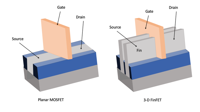
To comprehend the need for FinFETs, we must first understand the limitations of previous transistor technologies. Traditional planar transistors, such as the metal-oxide-semiconductor field-effect transistor (MOSFET), were plagued by power leakage and performance limitations as device dimensions shrunk. As the industry strived to reduce power consumption and enhance performance, an innovative transistor design became imperative.
Answer a few questions and get a recommended shortlist of foundries. Full scoring and a longer shortlist by email.
The journey towards FinFETs began in the late 1990s when engineers and researchers at the University of California, Berkeley, proposed a radical new transistor structure. Their idea was to replace the planar transistor design with a three-dimensional architecture to overcome the limitations of traditional planar MOSFETs, which led to the birth of FinFETs.
The development of FinFET technology marks a significant milestone in the field of semiconductor manufacturing. The term “FinFET” stands for Fin Field-Effect Transistor and refers to a three-dimensional transistor design that provides enhanced performance and power efficiency compared to traditional planar transistors. The history of FinFET technology can be traced back to the late 1990s when researchers at the University of California, Berkeley, proposed the concept of a vertical, multi-gate transistor structure. This breakthrough idea addressed the limitations of planar transistors in scaling down their size while maintaining good control over the flow of current. The researchers recognized that by using a fin-like structure as the channel region, they could achieve better electrostatic control, reduce leakage current, and improve overall transistor performance. In the early 2000s, major semiconductor manufacturers, such as Intel, IBM, and TSMC, embarked on intensive research and development efforts to refine and commercialize FinFET technology.
The working principle of a FINFET involves the use of a fin-shaped channel instead of a planar channel found in conventional MOSFETs. Unlike planar transistors, which have a flat channel, FinFETs employ a fin-shaped channel that protrudes vertically from the substrate. The channel is surrounded by gate electrodes on three sides, offering superior control over the transistor’s behaviour. The gate structure consists of a gate oxide layer, a gate electrode, and a gate insulator.
When a voltage is applied to the gate electrode, an electric field is created in the channel region. This electric field controls the flow of current through the channel. The unique design of the FINFET allows for better electrostatic control of the channel, reducing the leakage current and improving overall transistor performance.
Reduced Leakage Current: One of the primary advantages of FinFETs is their ability to significantly reduce power leakage. The vertical fin structure allows better control of the channel, resulting in reduced leakage current when the transistor is in the off-state. This improved control minimizes energy wastage and enhances power efficiency.
Enhanced Performance: FinFETs offer remarkable performance improvements compared to their predecessors. The three-dimensional structure allows for increased transistor density, enabling more transistors to be packed into a given area. This results in higher processing power and faster switching speeds, leading to improved overall device performance.
Scaling Possibilities: As electronic devices continue to shrink in size, the scalability of transistors becomes crucial. FinFETs have exhibited excellent scaling capabilities, allowing the semiconductor industry to continue its relentless pursuit of miniaturization. The design’s robustness in handling reduced transistor dimensions has been instrumental in maintaining the pace of Moore’s Law.
Lower Power Consumption: FinFETs operate at lower voltages than traditional transistors, leading to reduced power consumption. The improved control over the channel allows for better power management, resulting in longer battery life for portable devices and reduced energy requirements for larger systems.
Better Channel Control: FinFETs allow better control over the channel region, mitigating the short channel effects that plagued MOSFETs. The three-dimensional fin structure and the ability to modulate the width of the fin provides enhanced electrostatic control and reduced undesirable effects, enabling efficient scaling and improved performance. By adjusting the fin width, the threshold voltage and performance of the transistor can be fine-tuned enabling optimization for specific performance requirements.
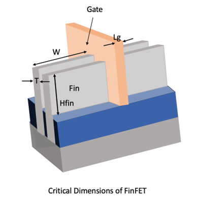
The following figure shows some of the critical dimensions of the FinFET that impact performance:
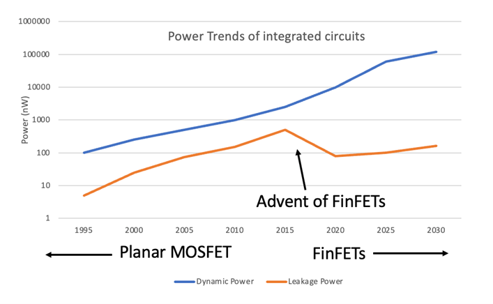
The advent of FinFETs has had a profound impact on a wide range of electronic devices. From smartphones and tablets to high-performance computing systems and IoT devices, FinFETs have become the go-to transistor technology for delivering power-efficient, high-performance solutions.
The semiconductor industry’s reliance on FinFETs has been instrumental in enabling technological advancements, such as artificial intelligence, machine learning, 5G communications, and autonomous vehicles. These transformative applications demand efficient processing capabilities, and FinFETs have provided the necessary foundation for such innovations.
Beyond FinFETs, there have been significant advancements in semiconductor technology that are shaping the future of electronic devices. Some of the notable technologies include:
Nanosheet FET (NS-FET): Nanosheet FET is an evolution of FinFET technology and is designed to further enhance transistor performance. Instead of a fin structure, it uses multiple ultra-thin silicon layers stacked on top of each other, forming a nanosheet. This architecture provides better electrostatic control and reduces current leakage, resulting in improved power efficiency and performance.
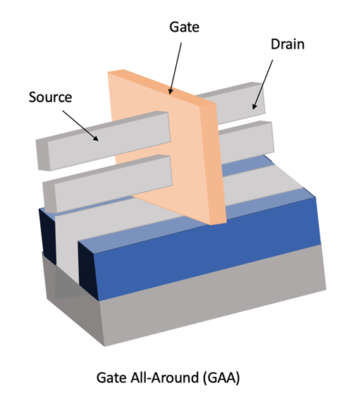
Gate-All-Around FET (GAA-FET): GAA-FET, also known as nanowire FET or nanoribbon FET, is an emerging transistor architecture that offers superior control over the channel region compared to FinFETs. In this design, the channel is surrounded by a gate on all sides, enabling better electrostatic control and reducing short channel effects. GAA-FETs offer excellent scalability, higher performance, and improved power efficiency.
Tunneling FET (TFET): TFET is a novel transistor architecture that leverages quantum mechanical tunneling phenomena. It replaces the traditional MOSFET (Metal-Oxide-Semiconductor Field-Effect Transistor) junction with a tunneling junction, which enables better control of the transistor’s behaviour. TFETs have the potential to operate at lower voltages, reducing power consumption, and can be used for low-power applications, such as mobile devices and Internet of Things (IoT) devices.
Carbon Nanotube FET (CNFET): Carbon nanotubes (CNTs) are cylindrical structures made of carbon atoms and possess excellent electrical properties. CNFETs utilize carbon nanotubes as the channel material, offering high carrier mobility and improved current density compared to traditional silicon-based transistors. CNFETs have the potential for high-performance applications and can operate at lower power levels.
Spintronic Devices: Spintronics, or spin electronics, is an emerging field that exploits the intrinsic spin of electrons in addition to their charge. Spintronic devices, such as spin field-effect transistors (SpinFETs) and magnetic tunnel junctions (MTJs), enable the manipulation of electron spins for data storage and processing. These devices have the potential to revolutionize memory technologies, leading to faster and more energy-efficient data storage and computing systems.
Neuromorphic Computing: Neuromorphic computing aims to develop hardware systems that mimic the structure and functionality of the human brain. It involves designing specialized circuits and architectures that can perform tasks such as pattern recognition, machine learning, and cognitive computing with exceptional efficiency.
These technologies represent the forefront of semiconductor advancements beyond FinFETs. While some are still in the research or early development stages, they hold the potential to drive significant improvements in performance, power efficiency, and functionality in future electronic devices.
FinFETs represent a significant milestone in the evolution of semiconductor technology. Their unique three-dimensional design, coupled with advantages like reduced power leakage, enhanced performance, scalability, and lower power consumption, has propelled electronic devices to new heights of efficiency and capability. As we continue to push the boundaries of technological innovation, the impact of FinFETs will remain pivotal in shaping the future of electronics.


