

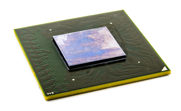
Flip chip , also known as “controlled-collapse chip connection” (C4), is an advanced semiconductor packaging technique that allows the direct attachment of a semiconductor chip, typically an integrated circuit (IC), to a substrate or circuit board. Unlike traditional packaging methods like wire bonding, in flip chip technology, the active side of the chip faces downward, and electrical connections are made through conductive bumps, usually made of solder or conductive polymers. These bumps serve as bridges between the chip and the substrate, forming reliable and high-density interconnections. Flip chip package is widely adopted in modern microelectronics and offers advantages in terms of miniaturization, performance, and thermal management.
The origins of flip chip package can be traced back to the mid-20th century when early experiments explored the concept of attaching semiconductor devices in this manner. However, it was not until later decades that significant advancements were made. Key milestones in the history of flip chip technology include:
During the 1960s-1970s, IBM played a pivotal role in the development of flip chip technology. They introduced Controlled-Collapse Chip Connection (C4), a method that used solder bumps for interconnection. C4 became synonymous with flip chip technology and set the foundation for its growth. Ongoing developments in materials science led to the refinement of solder materials, underfills, and adhesion layers, improving the reliability and performance of flip chip packages. As the demand for smaller, more powerful electronic devices grew, flip chip technology gained prominence in the microelectronics industry. Its advantages, including high-density interconnections and shorter signal paths, made it a preferred packaging solution. Today, flip chip technology is a cornerstone of semiconductor packaging, enabling the miniaturization and enhanced performance of electronic devices across various industries, from consumer electronics to aerospace and telecommunications. Its history reflects the continuous pursuit of smaller, more efficient, and higher-performing semiconductor packages to meet the ever-evolving demands of technology.
Flip chip technology involves several key components and materials that are essential for its successful implementation. These components work together to create reliable electrical connections and protect the semiconductor chip. Here are the key components of flip chip technology:
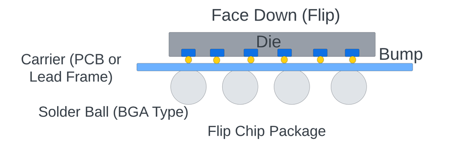
Figure 1: Flip Chip Package
Semiconductor Chip: (Die The die or the semiconductor chip contains the electrical components such as transistors, capacitors and interconnects of the integrated circuit. It is typically made from silicon and has bonding pads on its active side.
Bumps: Conductive bumps are small, raised structures on the chip’s bonding pads. They are made of materials like solder (e.g., tin-lead or lead-free) or conductive polymers. These bumps serve as the electrical connections between the chip and the substrate. Common bump materials include:
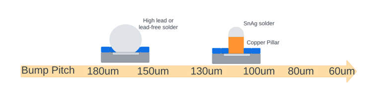
Figure 2: Bump Pitches for solder bump and copper pillars
Substrate or Interposer: The substrate, often a circuit board or another silicon wafer, provides a platform for the chip to attach to. It has matching bonding pads that align with the bumps on the chip. Common substrate materials include:
Underfill Material: Underfill is a material that is applied around the edges of the chip after it is attached to the substrate. It fills the space between the chip and the substrate, enhancing mechanical stability and protecting the assembly from environmental factors. It also provides thermal and electrical insulation.
The flip chip assembly process is a crucial step in flip chip technology, where a semiconductor chip is attached to a substrate or circuit board with the active side of the chip facing down. The process involves several steps to create reliable electrical connections and protect the assembly. Here’s an overview of the flip chip assembly process:
Preparation of the Semiconductor Chip: The semiconductor chip, often a silicon die, is prepared for attachment. The active side (with electronic components) typically faces downward.
Bump Formation: Conductive bumps are created on the chip’s bonding pads. These bumps are made of materials like solder or conductive polymers and serve as the electrical connections.
Preparation of the Substrate or Fluxing: The substrate, which could be a circuit board or another silicon wafer, is prepared for chip attachment. This step is also referred to as fluxing. It has matching bonding pads that align with the bumps on the chip.
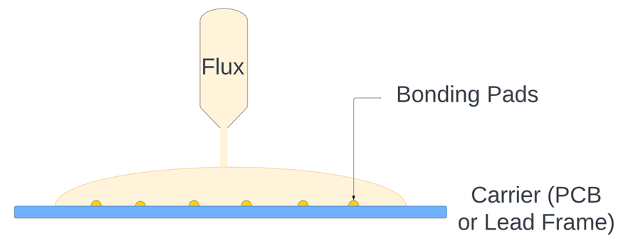
Figure 3: Fluxing or Preparation of the Substrate
Die Placement: The chip is flipped over so that the active side with the bumps faces downwards, and precise alignment equipment ensures that the bumps on the chip match the bonding pads on the substrate.
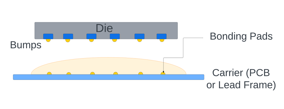
Figure 4: Die Placement
Reflow Process: The assembly is heated, typically through a reflow process, to melt the solder bumps. This causes the bumps to collapse and form reliable electrical connections. Reflow soldering has become the standard for attaching components in modern electronics manufacturing due to its precision, consistency and ability to handle the demands of miniaturization and high density circuit boards.
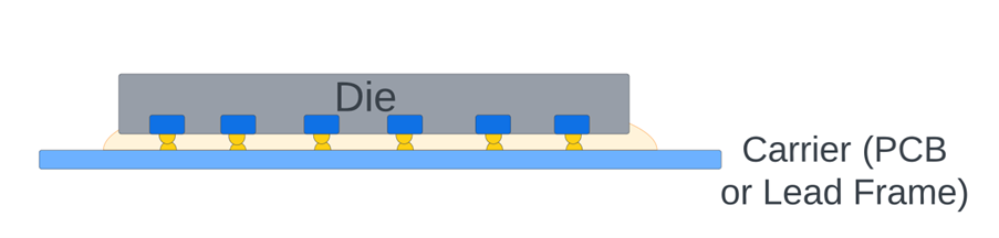
Figure 6: Reflow Process
Underfill Dispensing: An underfill material is applied around the periphery of the chip. The underfill encapsulates the assembly, providing mechanical stability, thermal insulation, and protection from moisture. It also enhances adhesion by providing a strong attachment for the chip.
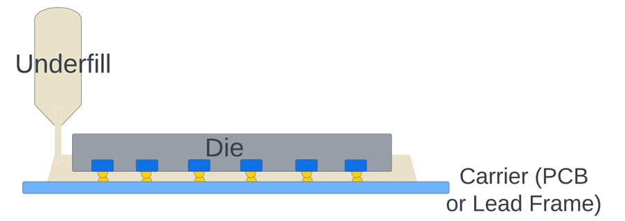
Figure 7: Underfill
Curing the Underfill: The underfill material is cured or solidified, ensuring it hardens and strengthens the assembly. Curing involves applying heat or ultraviolet (UV) radiation to the underfill material to change its physical properties and solidify it.
Testing and Inspection: The flip chip assembly undergoes various tests, including electrical testing, to verify the quality of the electrical connections. Non-destructive testing methods like X-ray inspection may be employed.
The resulting flip chip package offers advantages in terms of size, performance, and thermal management. It is a critical technology for high-performance and miniaturized electronic devices, such as microprocessors, memory chips, and high-frequency components. The precision and complexity of the flip chip assembly process contribute to its reliability and performance.
Flip chip technology offers several advantages over conventional packaging methods, especially in comparison to wire bonding. However, it also comes with certain disadvantages. Here’s a comparison of flip chip and wire bonding, which is a common conventional packaging method:
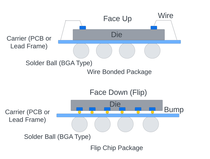
Figure 8: Wire Bonded vs Flip Chip Package
Flip chip technology offers numerous advantages, but it also comes with challenges and limitations. Some of the challenges and limitations associated with flip chip technology are as follows:
While flip chip technology is advantageous for many high-performance and miniaturized electronic devices, it is essential to carefully consider these challenges and limitations when choosing it for a specific application. Design optimization, material selection, and robust manufacturing processes are essential for addressing these issues and ensuring the reliability and cost-effectiveness of flip chip packages.
In conclusion, flip chip technology represents a transformative approach to semiconductor packaging that has redefined the possibilities of miniaturization, performance, and thermal management in modern electronics. By enabling high-density interconnections and shortening signal paths, flip chip technology has become instrumental in the development of compact, high-performance electronic devices. While it comes with complexities and challenges, ongoing research and innovations aim to address these limitations, ensuring that flip chip technology continues to help make our gadgets faster and smaller, making our lives more connected and convenient.
Get an indicative packaging cost range, then a detailed breakdown by email.
