

To make a rapid design start for your high-performance analog/mixed-signal IC prototypes, take advantage of ams OSRAM multi-project wafer (MPW) service. Reserve your place on the 2025 schedule.
When you need experienced and reliable manufacturing and a Europe-based supply-chain partner, ams OSRAM full-service foundry is the ideal choice for all customers. We invite fabless semiconductor companies and design houses to use our integrated circuit service for fabrication of IC prototypes for shared wafer fabrication. See the 2025 schedule for our fast and cost-efficient IC prototyping service, known as Multi-Project Wafer (MPW). By combining several designs from different customers onto a single wafer, participants can gain significant financial advantages as the costs for wafers and masks are shared.
Optimized for analog/mixed-signal ICs, our ams OSRAM MPW service makes available the full range of 180nm and 350nm specialty processes, including the recently introduced advanced 180nm CMOS technology. Customers can plan their participation well in advance, based on our already published schedule for planned tape-outs.
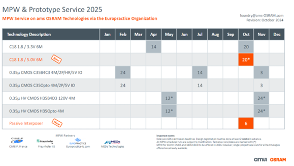
Overall, ams OSRAM will offer 15 MPW start dates in 2025, enabled by collaborations with our worldwide partner organizations, which includes CIME-P (formerly CMP) and Fraunhofer IIS via EUROPRACTICE. Customers located in the Asia Pacific and China region may also participate through our local MPW program partner, MEDs Technologies.
Our MPW runs are manufactured in our state-of-the-art 200mm fabrication facility in Austria, ensuring extremely low defect densities and high yields.
How to take advantage of the MPW service
Foundry customers must submit their completed GDSII-data on the specified dates. They will receive untested packaged samples or dies within a short lead-time. All process technologies are supported by the well-known PDK (process design kit) based on the Cadence design environment. The PDK comes with fully integrated silicon-qualified standard cells, periphery cells and general-purpose analog cells. Physical verification rule sets for PVS/Pegasus and Calibre, as well as precisely characterized circuit simulation models for the Spectre Simulation Platform, enable rapid design starts of complex high-performance mixed-signal ICs. In addition to standard prototyping, packaging services in ceramic, plastic or WL-CSP are also offered for ICs placed on our MPW.
What is new in 180nm CMOS MPW Offerings?
The latest updates in 180nm CMOS technologies emphasize enhancements in feature sets and process options, including:
C18 Process – 1.8V / 3.3V Variant: this configuration caters to battery-driven mixed-signal, digital, and analog applications. It is ideal for designs such as medical implants, power management ICs, IoT devices, and consumer electronics.
C18 Process – 1.8V / 5.0V Variant: this version expands the voltage range, enhancing its usability for devices requiring higher drive voltages. Applications include display drivers, precision analog circuits, and industrial controls.
As our technology offerings continue to evolve, they provide a powerful platform for modern semiconductor design. For example, design starts on a new high-voltage BCD (Bipolar-CMOS-DMOS) variant are already possible, with an MPW launch planned for next year. This variant is tailored for automotive, industrial, and power management applications, where robust high-voltage operation is critical.
Reliable semiconductor manufacturing and beyond. The full-service foundry partner you can rely on.
Why do fabless semiconductor manufacturers work with ams OSRAM? We help you to turn your ideas into IC solutions. Our dedicated team, extensive IP portfolio and high-accuracy simulation models, ensure effective development cycle. With ams OSRAM you also get a secure long-term supply chain through in-house wafer manufacturing, advanced testing facilities, strong partnerships, and full compatibility with the world’s leading semiconductor manufacturers.
Work with us from circuit design to backend needs and supply chain management. We act as your single point of contact, enabling rapid product releases. Simply select your preferred process technology, take advantage of our PDK, highly accurate circuit simulation models, and MPW service for quick prototyping.

From design to supply chain management: Work with us


