

Gallium arsenide (GaAs) technology is a type of semiconductor material used in the manufacturing of various electronic devices. It is known for its high electron mobility, which allows it to operate at higher speeds and with lower power consumption compared to other semiconductor materials such as silicon. GaAs technology is widely used in the production of optoelectronic devices such as lasers, LEDs, and solar cells, as well as in the field of wireless communication for its ability to transmit data at high frequencies. With its superior electrical and optical properties, GaAs technology continues to be an important advancement in the field of electronics.
Gallium Arsenide is slightly different from the conventional Silicon (Si) because of its semi-insulating property. The on state resistance of GaAs devices is low than Si because carrier mobility in GaAs is higher than in Si (almost six times that for silicon). It has high resistivity of 107 Ω.cm to 109Ω.cm which makes it suitable for fabricating high speed electronics and optoelectronics devices. This property also removes the need to provide insulation between devices on chip. GaAs devices operate faster as compared to Silicon devices for the same power dissipation and they dissipate less power than Silicon at the same speed. The speed advantage is obtained based on the fact that the average velocity of electron in intrinsic or extrinsic GaAs is higher than that of Si electrons. This material is desirable for the fabrication of devices. Since it possesses larger energy gap than silicon, that’s why devices made by GaAs can be operated at higher temperatures than silicon devices. Table 1 lists some of the important properties of GaAs. [1]
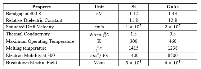
Table 1: Comparison of properties of Si and GaAs
In 1955, single crystal of GaAs had been grown and was used for building the photocells. The breakthrough in GaAs based devices came in 1965 when Carver Mead fabricated and tested first GaAs based field-effect transistor (MESFET). Researchers in U.S. and Europe kept on working in improving the efficiency of GaAs based MESFETs. Throughout the 1970s and 1980s, GaAs was used to construct a variety of circuits and components for everything from cellular phones to high-end computers. By 1970’s GaAs MESFETs emerged as a three terminal device with gate length of 1µm and found their applications in microwave amplification. The first major impact in commercial wireless market was made in early 1990’s by these GaAs MESFETs. They replaced their competitors Silicon BJTs because of their superior efficiency. In 1992, a new class of LED called the resonant-cavity light emitting diode RCLED was introduced using GaAs material. RCLEDs have higher emission intensities along the optical axis of the cavity, which allows for higher coupling efficiencies to optical fibers.
Today, GaAs is still widely used in electronics applications, although it has been surpassed by newer materials such as silicon germanium and indium phosphide. These new materials offer higher performance than GaAs, but since GaAs is an established technology, it remains popular among manufacturers.
GaAs continues to be used in a wide range of electronics applications, including cellular phones, wireless networks, and radar systems. Its unique properties make it especially suited for these types of applications, making it a mainstay in the world of modern semiconductor technology.
GaAs is one of the most popular materials for electronic components and devices due to its superior properties. It has an increased electron mobility, which allows it to transmit signals at higher speeds than other materials. In addition, GaAs offers a wider range of operating temperatures, allowing it to be used in smaller spaces with much less energy dissipated compared to other materials. This makes it an ideal choice for many applications such as radio frequency (RF) and microwave components, high-speed digital circuits, laser diodes, and more.
Furthermore, GaAs is highly resistant to radiation which makes it suitable for space exploration. Finally, its low cost compared to other materials makes it a desirable material for creating cost-effective and energy-efficient components. In short, GaAs offers numerous advantages over other materials, making it a popular choice for many uses. With all of its superior qualities and wide range of uses, GaAs is an optimal choice for creating components and devices with increased efficiency. Its wider operating temperature range allows it to be used in smaller spaces, while its radiation resistance makes it suitable for space exploration. At present, telecommunication sector is the largest user of GaAs electronic devices.
In addition, the low cost and ease of fabrication make it a great choice for cost-effective, energy-efficient components. All of these benefits make GaAs an ideal material for electronic components and devices. With its superior properties, GaAs is a great choice for creating cost-effective and energy-efficient solutions with excellent performance. The lower noise figures of GaAs reduce the filtering requirements as well as provided compact circuit design in full duplex analog cell phones.
Advantages seldom come without drawbacks. A brittle and expensive material is used for fabricating and processing the GaAs devices which is not an easy task, while processing and fabrication process of silicon is relatively quite easy. Another property that makes silicon devices more desirable is that it is cheap and mechanically robust than GaAs.
Although there are several advantages of GaAs over silicon, still it has not been possible to construct bipolar junction on GaAs that can compete with the Si ones. It is because of the impossibility of diffusing dopants into GaAs to form the p-n junctions as well as the slow mobility of holes. Somehow these problems have been overcome using heterojunctions bipolar transistors (HBTs) [2]. Other disadvantages include low thermal conductivity and poor mechanical strength as compared to silicon and thus at higher risk of facing thermal fatigue [3]. Power dissipated per unit area by silicon is three time for that of GaAs.
Silicon can also be protected and passivated by an easily grown SiO2 film, something that is not possible in case of GaAs. For isolating gate from the channel, silicon metal oxide semiconductor FET (MOSFET) use a layer of SiO2. As these devices can be made using p and n-channels so it is possible to permit complementary CMOS operation for low power consumption. MESFETs that use GaAs has the gate forward bias conduction limit of only 0.7V. In contrast to that, MOSFETs have bias limit approximately equal to supply rail. The limited gate voltages of MESFET degrade the noise margin of device thus greatly affecting the yield [4].
So far there are many advantages have been observed of GaAs, it has also some adverse effects on living beings. The workers in semiconductor industries inhaling these compounds have chances of cancer. So its manufacturing must be monitored and regulated by maintaining clean rooms for the workers [5].
Since 1985, insertion of GaAs ICs in electronics has been a trend. These applications inspired much of the earliest work in GaAs ICs. Performance requirements of these devices proved to be a powerful driver for GaAs ICs. The total market for GaAs electronic devices in 1999 was US$3602 million which was risen to US$11009 million till 2004. Hence an overall growth rate of 24% was observed [6].
The properties associated with GaAs like high electron mobility, fast emission and absorption of light, good heat resistance and ultra-high frequency will make it an integral part of modern semiconductor devices used in telecommunication systems for 5G technology. Not only the telecom industry will take advantage of this material but also the solar panels can use its photovoltaic property for their production.
The shift of focus of RF or microwave market from military to commercial side, will bring more challenges and opportunities for GaAs ICs. On the other hand, lower cost expectations and lower frequencies will demand more aggressive comparison for GaAs ICs with silicon. These changing trends will make a dynamic market place for GaAs ICs.
In communication market, the future of GaAs devices in so promising with continued applications in optical fiber communication systems. Under development are a NASA search rescue program for navigation and rescue, phased-array antennas and advanced commercial aircrafts for communications.
If we look at the GaAs based devices as front-end transducers of high frequency, coupling mobile telephones, 802.11, Bluetooth, and the mostly untapped transportation markets, what more do we need to convince ourselves for an unlimited market potential.
MMIC Technology for Low Cost W-band Transceivers
Flip chip bonding (FCB) technology is used in radar systems and wireless local area network systems at frequencies of 76 GHz and 60GHz respectively. The schematic cross section for FCB multilayer MMIC is shown in the Figure 2.
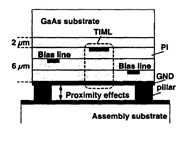
Figure 1: A schematic cross section of the FCB multi-layer
It consists of four metal layers and polyimide (PI) layer which is fabricated on GaAs substrate. Ground metal covers the MMIC surface and can screen face-down MMICs from assembly substrates hence reducing the proximity effects. Thin-film inverted microchip lines act as main lines and these are formed by the first layer line and the top ground metal on the GaAs substrate. Second and third lines act as the bias lines. Chip area can be reduced by lowering the line spacing for impedance matching circuits, but in mm-wave frequency range it results in cross talks among signal lines. This may affect the MMIC performance badly.
Electromagnetic coupling between the transmission lines is reduced by inserting 2-µm thick PI between GaAs substrate and signal line. Additionally, in order to reduce the radiation of the electromagnetic field from the signal lines, the PI thickness between the signal line and the ground layer is kept as thin as feasible. However, because of the narrower line, the thinner PI increases the insertion loss of the 50 ohm lines. Then, using electromagnetic simulation, it can be concluded that the ground layer must be 6 pm thick in order for signal lines to have the proper characteristic impedance and insertion loss.
Pseudo-morphic-High-Electron Mobility Transistor (pHEMT)
One design example of chips that use GaAs is the pseudomorphic high-electron mobility transistor (pHEMT) design. This design allows for higher frequency operation, lower noise performance and better thermal stability than traditional transistors. The pHEMT design also has less resistance in comparison to other designs, allowing for more efficient power dissipation. Additionally, GaAs pHEMT design allows for the fabrication of miniature transistors on a single chip, allowing for more complex circuits to be constructed in less space. This makes chips that use this design ideal for applications where size and performance are important factors.
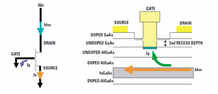
Figure 2: pseudomorphic high-electron mobility transistor (pHEMT)
Here is the list of names and website links that manufacture wafer fabs of GaAs
References
[1] POWER. ELECTRONICS. Converters, Applications, and Design. SECOND EDITION. NED MOHAN. Department of Electrical Engineering. University of Minnesota.
[3]https://books.google.com.pk/books?id=NErRJEn3hRUC&pg=PA401&dq=drawbacks+of+GaAs+devices&hl=en&sa=X&ved=2ahUKEwjn-I_rv-T7AhVwTKQEHUZ3BycQ6AF6BAgGEAI#v=onepage&q=drawbacks%20of%20GaAs%20devices&f=false
[5] https://www.factmr.com/report/gallium-arsenide-market
[7] https://ieeexplore.ieee.org/document/1049022


