

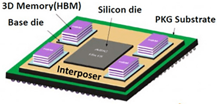
High-bandwidth memory (HBM) is a JEDEC-defined standard, dynamic random access memory (DRAM) technology that uses through-silicon vias (TSVs) to interconnect stacked DRAM die. In its first implementation, it is being integrated with a system-on-chip (SoC) logic die using 2.5D silicon interposer technology.
In June 2015, AMD introduced its Fiji processor, the first HBM 2.5D design, which comprises a graphics processor unit (GPU) connected with four HBM stacks using a silicon-based interconnect. The Fiji processor is powering AMD’s latest generation of Radeon Fury graphics cards for high-performance gaming. This event was the turning point for HBM, opening the floodgates for system integrators to adopt HBM as a memory solution for high-bandwidth, low-power products. In addition to graphics, HBM is being used in high-performance computing (HPC), data center and networking applications.
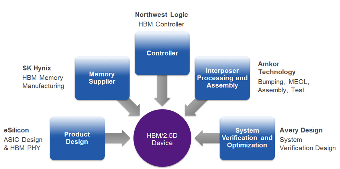
SK hynix Inc., Amkor Technology, Inc., eSilicon Corporation, Northwest Logic and Avery Design Systems have joined forces to offer a complete HBM supply chain solution that is delivering and supporting customer HBM designs now.
In this open supply chain collaboration, SK hynix provides the HBM stack. eSilicon is the application-specific integrated circuit (ASIC) vendor for the SoC, providing the HBM physical interfaces (PHYs) and associated services, and is also the overall HBM module integrator. Northwest Logic provides the HBM controller intellectual property (IP) for the SoC. Avery Design Systems provides the HBM verification IP. Amkor integrates the SoC, HBM stack and interposer into a 2.5D assembly, and tests, packages and ships it to the customer (Figure 1).
The five companies recently sponsored a seminar to promote their efforts and explain how this supply chain works. Attendee feedback was very positive and included the following comments:
This white paper explains HBM’s value proposition, and how these five companies make it easy for system and integrated circuit (IC) designers to access the many benefits this technology offers.
HBM is a JEDEC-defined standard DRAM stack. It is integrated with an SoC using a fine-pitch interposer. The first HBM-based product went into production in early 2015. Many companies are already using HBM to create very-high-bandwidth, low-power products (Figure 2).
HBM was developed by JEDEC and its member companies to meet the needs of applications in which memory bandwidth needs exceed the capabilities of traditional memory approaches like DDR4 and GDDR5. A single HBM stack provides bandwidth equivalent to 16 DDR 4/3 DIMMs. Multiple HBM stacks can be connected with a single SoC in an HBM 2.5D package design.
HBM has emerged as the leader in customer adoption over competing technologies due to its low-power capabilities, JEDEC standardization and availability from multiple sources. SK hynix is the first memory manufacturer to ramp HBM to production.
In response to this market demand, SK hynix, eSilicon, Northwest Logic, Avery Design Systems and Amkor Technology have put together an end-to-end supply chain for HBM/2.5D designs.
SK hynix began to develop HBM technology in 2011 when it became clear that memory density and bandwidth scaling would be critical for next-generation architectures. Graphics, HPC, networking and data center applications were experiencing a memory bottleneck due to a performance discrepancy between CMOS logic and DRAM.
TSV technology is the enabling interconnect technology used in HBM that allows DRAM memory to overcome existing bottlenecks. TSVs run interconnects through the die, making it possible to stack a higher number of die without needing to run wire bonds from pads to the package, thereby reducing the overall package size of the DRAM device.
HBM overcomes all DRAM bandwidth challenges. Low speed-per-pin and input/output capacitance (Cio) reduce power consumption and increase efficiency. Usually, power and bandwidth go hand in hand. However, because HBM is designed as an in-package memory that sits next to the processor or ASIC (SoC) on top of an organic or silicon interposer, driver size and capacitance is minimized. Bandwidth is now a product of I/O speed. In fact, HBM provides the highest bandwidth per unit area when compared with other DRAM memories.
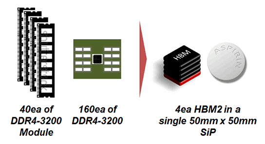
To provide 1 Tb/second of memory bandwidth using conventional DRAM such as DDR4 requires a tremendous amount of space on the printed circuit board (PCB): 160 DDR4 components take up 15,600mm2 of the PCB, versus 4 HBM2 components, which take up 384mm2 (Figure 3).
Further, from a raw bandwidth perspective, the 2 Tb/second of bandwidth that a single HBM provides would require 40 DDR PHYs on the ASIC. This takes up 300mm2 of ASIC real estate compared with 12mm2 needed to accommodate a single HBM.
To ensure quality and reliability, a programmable built-in self-test (BIST) engine to test, detect and correct failures was added. System architects appreciate the ability to do post-package repair according to the IEEE 1500 standard.
The HBM supply chain is ready to support designs. Seven test vehicles have been taped out. Two production designs being developed by eSilicon for HPC and networking, one at 28nm and one at 14nm, expect to ramp to volume in 2016. Many additional customer designs are underway.
Going forward, SK hynix plans to redesign HBM to accommodate vertical stacking. The company is also exploring a low-power ARM-based SoC that could theoretically support an HBM stacked on top for mobile applications.
eSilicon has been specializing in 2.5D interposer designs since 2011 with its modular Z-axis integrated circuit (MoZAIC™) program. The MoZAIC program focuses on enabling the IP, design capability, packaging/test methodologies and supply chain needed to ensure the lowest-risk, highest-performance device development.
Seeing the need for an ecosystem to support HBM integration, SK hynix first came to eSilicon as an ASIC vendor. eSilicon then invited Northwest Logic, Avery Design Systems and Amkor Technology to become part of this dedicated supply chain, because each brought a different element to the table, without any conflicts or overlap.
eSilicon developed its first 2.5D device using first-generation HBM in 2012. Since then, eSilicon has been actively developing and offering organic and silicon interposers and other IP and technologies needed in this space. This includes HBM PHYs as well as delay-locked loops (DLLs) and I/O libraries, catering to a wide variety of customers and market segments from 28nm to 14nm/16nm (Figure 4).
As the ASIC vendor and system integrator, eSilicon works with major computing and network vendors to support ASIC design by determining what parts work well together to achieve desired functionality. eSilicon also designs the interposer and package to deliver a turnkey solution.
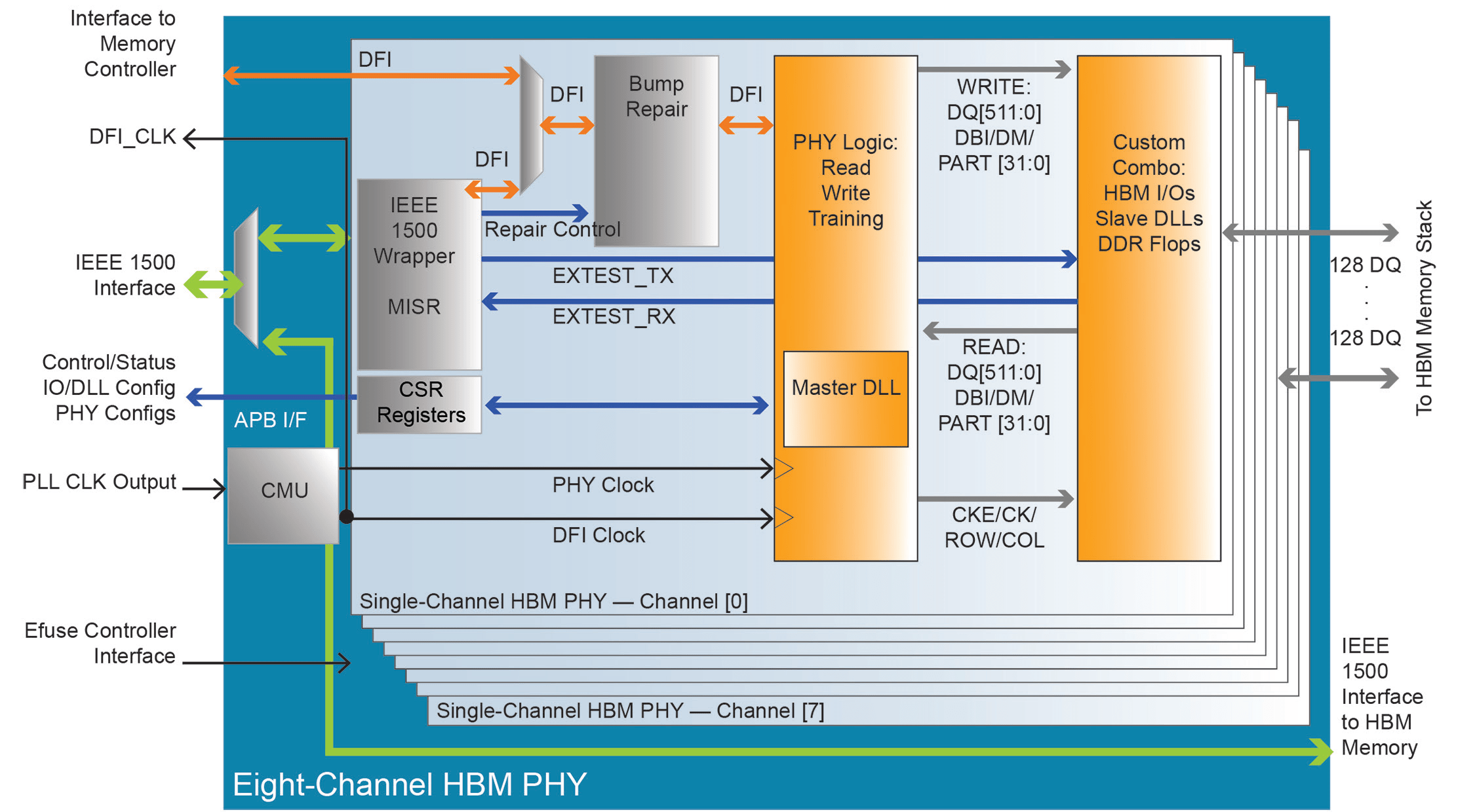
Northwest Logic provides a high-performance, highly configurable HBM controller core. As shown in Figure 5, this core consists of a base HBM controller plus a variety of add-on cores.
The base HBM controller uses all of the available HBM features including pseudo channels, look-ahead activates/pre-charges, single-bank refreshes, etc., to ensure that the maximum possible bandwidth can be achieved in a targeted user application. The HBM controller can be configured in a variety of ways, including a single/dual user interface, half/full-rate operation, etc. This enables the user to select the configuration that best meets their design needs.
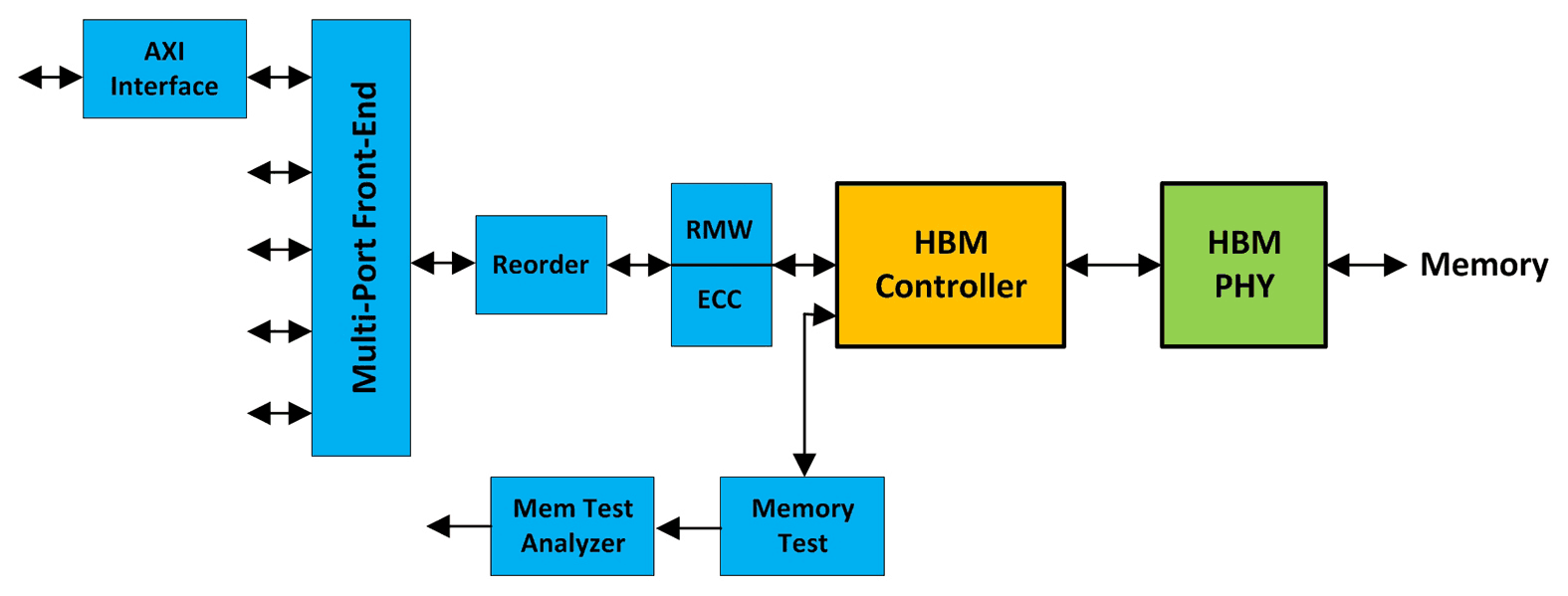
The base HBM controller can be optionally used with a variety of add-on cores. These add-on cores extend the functionality of the controller to support multiple ports, transaction reordering to maximize bandwidth, ECC and advanced test capabilities. Only the add-on cores needed by the customer are included in the delivery, minimizing the size and complexity of the controller.
The advanced test capabilities allow the HBM controller to perform a complete set of write-then-read transactions to the HBM stack with predefined, user-defined and random data and address patterns. This enables comprehensive bring-up and production system testing to be performed and easily analyzed.
Northwest Logic delivers the HBM controller fully integrated and verified with the eSilicon HBM PHY. This includes eight instantiations of the HBM controller (one for each HBM channel). Northwest Logic uses its full-featured verification environment, which includes interface test benches and HBM models from Avery Design Systems and the memory vendors to comprehensively verify each customer delivery over a full range of HBM memory configurations and traffic patterns.
As of March 2016, the HBM controller is being used in seven customer designs and multiple test chips. These designs include HPC, design center and networking applications that have a wide range of feature requirements and traffic scenarios. These real-world uses have enabled Northwest Logic to optimize the HBM controller so that it achieves the highest application bandwidth possible, and supports the broadest range of customer applications.
Avery Design Systems develops and delivers verification IP (VIP) solutions including models, protocol checking, compliance test suites and support services. VIP is a behavioral model that implements standard protocol and allows system designers to simulate a device without having to build prototypes.
For example, when designing a high-end system router that uses memory to store data packets and run various routing, filtering and encryption algorithms, Avery Design Systems’ memory model VIP helps verify that the memory subsystem is functioning correctly and efficiently. Designers run a chip-level simulation while connected to the memory model, and can test traffic through the router chip to see how it operates to the memory chip module standards.
As part of this open supply chain, Avery provides HBM models that enable HBM-based SoC and PHY designs to be robustly verified and performance-optimized quickly and effectively.
While memory suppliers provide models for free, they offer minimal capabilities. Avery Design Systems offers a more complete solution that includes robust and flexible bus functional models (BFMs), protocol checking and analyzer trace logs, functional coverage, performance analysis, SoC/IP compliance test suites, an intelligent scoreboard, integration with a native system Verilog test bench, and much more, including full customer service and support.
Tuning a system involves the memory controller, system interconnect, custom engines, software on embedded processor and a memory interface that describes how fast information is sent into and out of the memory. It is important to make sure the algorithm runs quickly, has the lowest latency possible and accesses the memory system correctly.
Avery’s HBM verification IP solutions support HBM2 and spec revisions from JEDEC and IEEE 1500 test ports. The company supports a behavioral BFM PHY monitor and matches the PHY interfaces to ensure it adheres to PHY standards. An optional memory controller BFM and compliance test suite generate traffic scenarios to further verify the PHY. The HBM memory model BFM supports all test bench configurations, configurable number of channels, density, banks and operating speeds, and the IEEE 1500 port commands. Additionally, as debugging is important for analyzing designs, the HBM model generates protocol analyzer logs; performs protocol and timing checks, function coverage, and performance analysis including: DQ usage, bandwidth, bank analysis, and command latencies to identify memory subsystem and SoC interconnect performance issues and inefficient memory page allocation.
Once the system architect decides to select HBM versus other memory alternatives such as DDR4 and Hybrid Memory Cube (HMC), the register transfer logic (RTL) design and verification phase begin yielding a complete RTL model of the chip comprising embedded processors, custom functions, engines, system interconnect, a network on a chip, etc.
In the case of an HBM 2.5D design, the RTL designer can rely on Northwest Logic to provide a synthesizable RTL memory controller IP; eSilicon provides PHY design including a behavioral model of the PHY; and Avery Design Systems provides the HBM memory model. SoC RTL verification then targets generating system memory traffic through the simulated system to make sure the algorithm is functioning correctly and providing the right result with good performance. The HBM model is programmed to inject various errors to make sure the system can log it and perform error recovery.
The implementation and verification teams work in parallel paths. Once the verification team is through with its simulations, a gate-level netlist is created. eSilicon then implements the netlist into a chip layout and works with the fab to implement place and route, testability, and final sign-off and tapeout.
When the design, simulation and chip fabrication steps are complete, Amkor Technology performs the 2.5D device assembly, test, packaging and shipment.
Amkor Technology is an outsourced semiconductor assembly and test service provider and the leader in advanced system-in-package (SiP) technology. Amkor has been developing 2.5D and 3D integration technologies since 2006, resulting in a fully qualified production line, middle-end-of-line (MEOL) and assembly for 2.5D and 3D technology. The MEOL process flow includes interposer bumping on the front side, TSV reveal on the back side, followed by redistribution layer, micro-bumping and assembly of the ASIC and HBM stack on the interposer. It also performs interim and final test as directed by the customer. The MEOL and assembly production lines at Amkor are fully qualified and ramping new HBM/2.5D products to meet customer forecasts.
All of the bill of materials content for the HBM/2.5D designs are consigned to Amkor by eSilicon, including: the foundry-manufactured TSV interposer; the memory cube from SK hynix; and the 300mm ASIC wafer from the foundry. One benefit of working in partnership with eSilicon and SK hynix is that all parts are qualified as compatible with Amkor processes. Amkor performs interposer MEOL, as well as fine-pitch copper pillar bumping of the ASIC wafer to better control compatibility with downstream assembly processes.
Get a higher resolution image here.
Interposers are fabricated at various foundry suppliers, typically based on 60nm back-end-of-line technology and via-middle TSV integration. TSV formation from different suppliers has converged on similar via manufacturing, resulting in consistent TSV quality, allowing Amkor to use a single MEOL process flow for multiple TSV suppliers. This promotes low cycle time and reduced cost with consistent reliability. Amkor continues to partner with foundries to facilitate new sources and extend cost-reduction initiatives.
SK hynix HBM is qualified with Amkor’s assembly process for 2.5D integration. Lastly, all the major foundries are qualified for logic devices using Amkor’s fine-pitch copper pillar bumping.
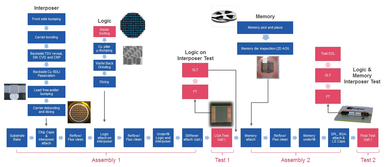
Amkor supports multiple assembly flows to provide flexibility in HBM/2.5D designs. These include 2.5D chip-on-substrate (CoS) assembly, 3D CoS assembly and 2.5D/3D chip-on-wafer (CoW) assembly. Flexible assembly options allow customers to make critical architecture decisions that best support their product requirements, including interim interposer test of interposer and ASIC before committing HBM devices to the assembly flow. 2.5D and 3D CoS assemblies are production-ready.
The CoS approach involves assembling each component one by one, which allows the logic and interposer to undergo interim tests before the memory is attached, so yield is assured before committing the memory to the stack. Back-side process steps for the interposer and logic die can take place concurrently, as both components are processed through parallel production lines before being staged for assembly. After the interposer is attached to the substrate, the logic die is attached to the interposer and prepared for an optional interim test step. Both functional test (FT) and system-level test (SLT) are supported. Next, HBM is attached to the rest of the subassembly and then final assembly is completed. Final FT and SLT are performed, and the parts are packaged and shipped to the customer (Figure 6).
2.5D CoS is active with many customers. It targets GPU, HPC, networking and server applications. 3D CoS and 2.5D/3D CoW are being deployed for memory customers.
Amkor’s production line will allow more customer penetration into HBM/2.5D products, which in turn reduces costs and improves efficiencies. Applications include GPU, networking/communication, memory systems, and server and HPC platforms.
HBM provides memory bandwidth far beyond what is available with traditional memory devices, such as DDR4 and GDDR5, at attractive power and cost.
The introduction of AMD’s HBM-based Fiji product not only proves the manufacturability of HBM 2.5D designs, but the marketability of such a product.
In this paper, five leading-edge companies have demonstrated the capabilities of an open-collaboration HBM/2.5D supply chain that is fully ready to take on designs for high-volume production.
eSilicon’s HBM PHY, Northwest Logic’s HBM Controller and Avery Design Systems’ HBM VIP models are all fully verified. Additionally, SK hynix’s HBM stack is fully qualified, as are two interposer suppliers. Amkor’s TSV MEOL line is mature and in production, with >98% yields and CPKs of over 1.3. Several test vehicles have been taped out. Additionally, two HBM production designs for HPC and networking, one at 28nm and one at 14nm, expect to ramp to volume this year.
Clearly, the time has come for HBM 2.5D designs, and the players are in place to help your company compete in this competitive landscape. Start your HBM 2.5D design today.


