

Shipping wafers involves more than simply placing them in any box; it requires specialized knowledge and handling techniques. Choosing the right packaging solutions, understanding logistics, and maintaining stringent environmental controls are all pivotal to safeguarding these fragile materials. Innovations like eLX™ and ePRO™ products are redefining the standards for wafer shipping.
This article will guide you through the essential steps in effectively shipping wafers, from selecting the right packaging to controlling external factors like temperature and shock. By implementing best practices and exploring advanced solutions, you can ensure safe delivery and maintain the quality of your valuable semiconductor components.
Understanding the importance of proper wafer shipping is crucial for the semiconductor industry. Wafers are delicate and prone to breakage. Thus, their transportation demands specialized services and packaging solutions.
Key Points to Ensure Safe Wafer Shipping:
Companies invest in proper shipping methods to lower freight spending and cost of ownership. Semiconductor manufacturers rely on safe transportation to ensure their electronic components and devices arrive intact. To meet these demands, shipping companies provide tailored solutions, ensuring delicate, thinner wafers are shipped without compromise.
Shipping delicate wafers in the semiconductor industry demands specialized handling products. Ensuring wafer integrity is crucial to avoid breakage during transit. Here’s how to choose the right handling products:
1. Wafer Shippers
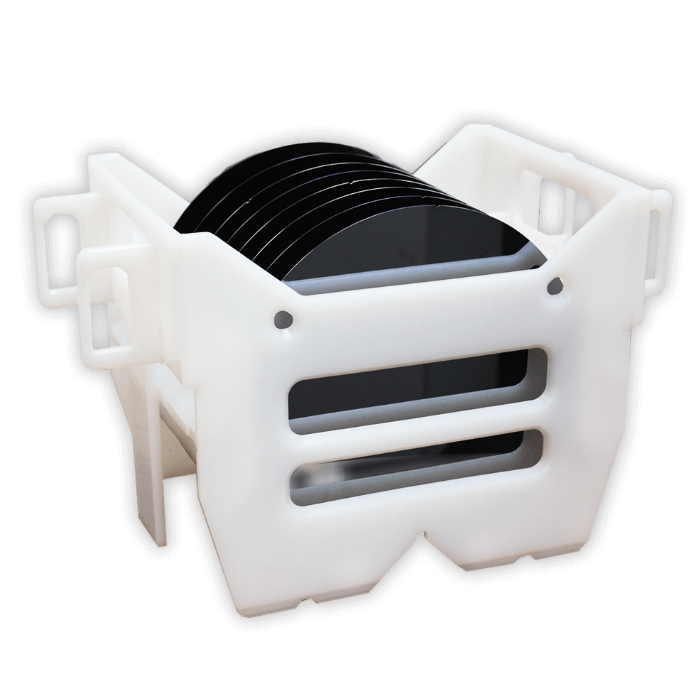
2. Wafer Boxes
Select boxes with a wide range of sizes to accommodate varying thicknesses, including thinner wafers. Ensure they prevent particle generation and allow for safe transportation.
3. Secondary Packaging
Packaging systems protect the electronics used in many devices. For the best results, work with logistics companies offering specialized services. They help semiconductor manufacturers minimize costs and maintain a low cost of ownership. By using these packaging solutions, you safeguard electronic components effectively during shipping.
Shipping wafers is crucial in the semiconductor industry. These fragile components must reach their destination without damage. Logistics companies play a vital role in handling this task. They provide a wide range of specialized services to ensure safe transportation.
The logistical process includes selecting the right wafer shippers. This means considering wafer shipping boxes and the level of protection they offer. Horizontal and Clamshell Style Shippers are popular for maintaining wafer integrity.
Secondary packaging, such as wafer separators, provides an additional layer of safety. It’s important for keeping delicate and thinner wafers secure. Shock indicators can be added to monitor transport conditions. Logistics companies also look at reducing cost of ownership and freight spending.
Inbound logistics is essential for semiconductor manufacturers. It involves managing raw materials and electronic components before production. These parts need to be handled with care to avoid wafer breakage.
Efficient inbound logistics ensure timely delivery and inventory control. This helps maintain the quality of incoming wafers. Shipping companies should focus on minimizing particle generation that can occur during handling.
Effective inbound logistics also require close collaboration between manufacturers and shipping companies. This partnership ensures a streamlined supply chain and consistent wafer integrity.
Effective distribution strategies are key to wafer shipping. A well-planned approach ensures wafers reach their destinations on time and in perfect condition.
Here’s a simple table summarizing key shipping strategies:
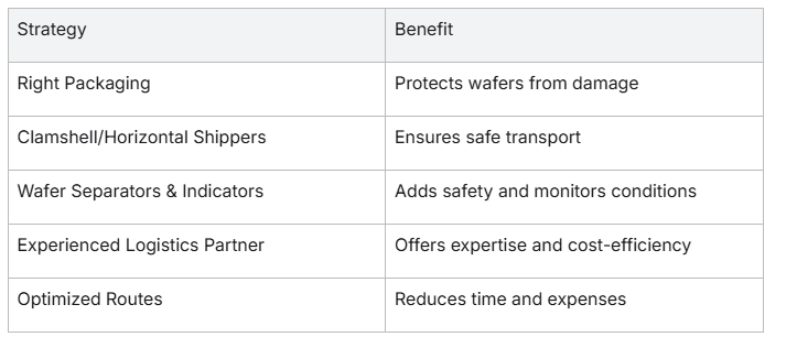
By employing these strategies, semiconductor manufacturers can enhance wafer integrity during shipment. This leads to efficient distribution and effective wafer shipping endeavors.
Shipping wafers requires careful attention to temperature and humidity. These factors can impact wafer integrity, essential for semiconductor manufacturers. Companies need a level of protection that preserves wafers’ delicate nature.
Proper temperature and humidity control reduce wafer breakage and particle generation. It’s crucial to maintain stable conditions during shipping. This ensures that wafers reach their destination in perfect condition, ready for use in electronic components.
To maintain optimal conditions, follow these best practices:
Shipping delicate wafers requires precise handling. Implementing shock control measures is crucial to maintain wafer integrity during transit. The semiconductor industry relies on specialized services and packaging to protect these sensitive electronic components. Using the right wafer boxes, such as clamshell style shippers or horizontal wafer shippers, helps ensure safe transportation. Shock indicators, tip indicators, and shock sensors add an additional layer of protection, reducing wafer breakage and safeguarding the investment in raw materials and electronic devices
.
Tip indicators play a vital role in shipping fragile wafers. These devices are placed on the packaging to detect if the box has been tipped over. When shipping companies use tip indicators, they can determine if the level of protection is compromised. This helps manufacturers of semiconductors inspect shipments on arrival. If a tip indicator shows that the package was mishandled, logistics companies can improve their services, ensuring wafers arrive undamaged.
Shock sensors are designed to detect and record impacts during wafer shipping. They provide valuable information about the conditions faced by wafers in transit. With shock sensors, shipping companies can monitor any forceful impacts the package encounters. This data helps reduce wafer breakage and ensures thinner wafers are shipped without damage. By using shock sensors, semiconductor manufacturers can enhance wafer integrity and reduce freight spending, ultimately optimizing the cost of ownership.
Shipping wafers requires careful planning to protect the delicate and often thin materials. In the semiconductor industry, the choice of wafer delivery options is crucial. Selecting the right shipping container ensures wafer integrity and prevents breakage during transit.
When shipping wafers, two common methods are clamshell style and horizontal wafer shippers. Each method offers unique benefits:
The chosen shipping company should have experience in handling electronic components and devices. It’s critical to use logistics companies that offer specialized services and have a proven track record in wafer shipping. Using shock indicators and an additional layer of protective materials can further safeguard the wafers.
Overall, understanding the nuances of each shipping option helps manage freight spending efficiently while maintaining wafer quality.
When shipping wafers, the integrity of each wafer is crucial. These delicate wafers are integral to the semiconductor industry, and improper handling can lead to wafer breakage. To protect them, robust packaging is essential. Wafer shipping boxes are designed to provide a high level of protection. They help absorb shocks and prevent any damage during transportation. Shock indicators can be attached to these boxes to monitor any impacts, ensuring the wafers remain safe.


