

This article provides an overview and description of a typical IC layout process. Its describes the various steps within IC layout and the relationship between each step.
IC layout refers to the backend design cycle. If there’s just one aspect that distinguishes the backend design from frontend design, then it would be- delay. Frontend design, while being cognizant of the logic delays and speed, largely ignores it for majority part of the RTL coding and verification. While, on the other hand, physical design sees real delay right from the very beginning.
IC layout flow is further sub-divided into the following:
Synthesis
Synthesis reads in the RTL code (.v or .sv files) along with physical libraries of the standard cells that may contain- delay information (.lib files), physical dimensions and metal layer information within the cell (.lef files) and other constraint files to convert the behavioral or dataflow code into real physical standard cell gates. Note that there are many possible implementations for 2:1 Multiplexer, and Synthesis is responsible to do an educated trade-off with performance, power and area to come up with the best implementation considering these constraints. As an example for the 2:1 Multiplexer, one possible implementation is below:
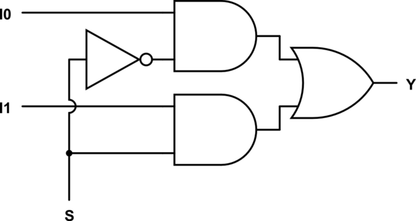
Figure 1: Gate level implementation of 2:1 Multiplexer
Floorplanning
Floorplanning step formalizes and refines the floorplan that was first conjured up during the architecture planning step. In this step, the entire die area is divided into physical partitions, and their shapes are molded while keeping in mind the area requirements, the flow of top level data and control buses, possibility of any future growth. Pins and ports are assigned a rough location, which can further be refined depending on the Place and Route results.
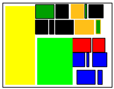
Figure 2: Floorplanning the blocks relative to each other. Image Courtesy: Andrew Kahng, UCSD
It’s quite common for physical design engineers to work on more than 1 floorplan in parallel, and try to evaluate which one works best for overall design QoR (Quality of Results). This is usually the most critical step in physical design cycle, and requires multiple iterations. Any additional time spent here is worth it considering its long lasting implications on routing congestion, cell density, timing QoR and DRCs.
A robust power grid delivery- which addresses static and dynamic IR drop is also a critical function of the floorplanning step.
Placement
During placement, all standard cells are placed in legal locations on site rows. The aim of this step is to minimize the wire length, while ensuring optimal placement that will help faster timing convergence.
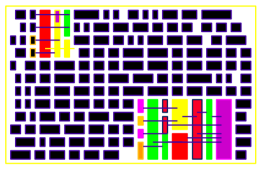
Figure 3: Standard Cells arranged on site rows. Image Courtesy: Andrew Kahng, UCSD
No real routes are laid during this step. Placement estimates routing through a step called Global Routing, where it estimates the total wire length and global route congestion. Many modern placement engines have the capability to take into account the switching activity from SAIF or VCD files, and try to optimize placement for achieving lower dynamic power.

Figure 4: Placed design. Image courtesy: Andrew Kahng, UCSD
Clock Tree Synthesis
Till now, clock network was ideal. During clock tree synthesis, clocks are propagated and the clock tree is synthesized using clock buffers. The major goals of this step is to achieve optimal clock latency while minimizing clock skew. There are many proposed algorithms to design an optimal clock tree- H Tree, Steiner Tree etc. In addition to this, one may choose Clock Tree Mesh, Multi-source Clock Tree Synthesis or traditional Single Point Clock Tree Synthesis which offer trade-offs for dynamic power, routing resources and OCV adjustment due to common clock path.
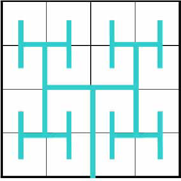
Figure 5: Typical H tree clock distribution. Image Courtesy: Research Gate
Clock being the signal with highest toggling frequency in the design, clock buffer tree accounts for over 75% of the dynamic power dissipated in an ASIC. Architecture may support clock gating to turn off idle parts of the chip to save dynamic power.
Detail Routing
With all instances placed and clocks routed, now it’s time to route the signal nets. Modern process supports 10-12 metal layer stack, with M0-M1 reserved for standard cell routing. The algorithm used for detail routing is usually a glorified maze router with added constraints to ensure faster run-times. The metal resources are divided into tracks which are the legal locations for metal routes. Aim of detail routing is to ensure minimum detours because these may have implications on timing, and to ensure minimum DRC (Design Rule Check) violations like opens, shorts etc. This step performs multiple search and repair loops (10-20) to keep the overall DRC count low.
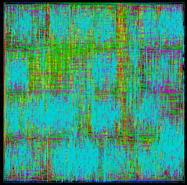
Figure 6: Routed Design. Image Courtesy: Andrew Kahng, UCSD
Physical and Timing Verification
While logic verification ensures correct functionality, physical verification ensures correct layout. There’s been an increase in Physical Verification checks which includes- DRC (Design Rule Checks), LVS (Layout versus Schematic), Electromigration, Electro-static discharge violations (ESD), Antenna violations, Pattern Match (PM) violations, Shorts, Opens, Floating nets etc. It is important to track these violations in parallel with the Place and Route flow to avoid any surprises just days before tape-out.
Timing Verification verifies that the chip runs at the specified frequency by ensuring setup and hold is met for all timing paths in the design.
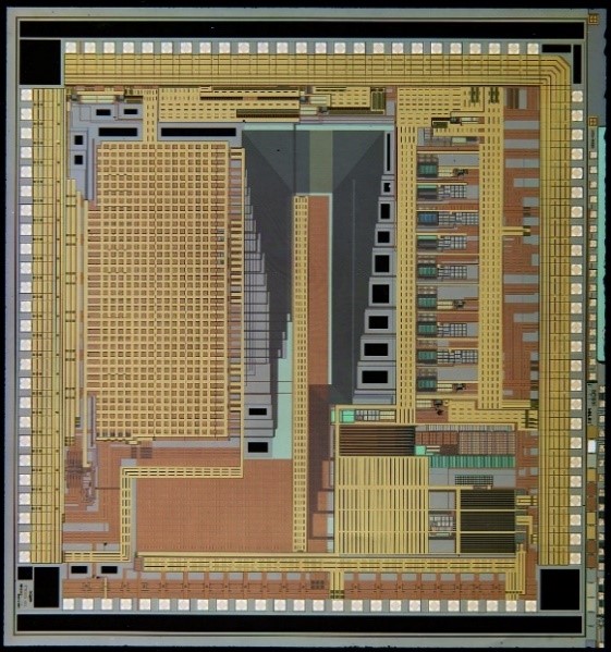
Figure 7: FRICO ASIC, 350 nm technology


