

Integrated circuit packaging technologies have evolved throughout the years to the point where hundreds of IC package types are available today.
Most applications will require the more general, single-element packaging for integrated circuits and the other components such as resistors, capacitators, antenna etc. However, as the semiconductor industry develops smaller and more powerful devices, a ‘system in package’ (SiP) type of solution is becoming the preferred choice, where all elements are placed into a single package or module.
![]()
While IC package types can be easily categorized into lead-frame, substrate or wafer-level packages, selecting a package that will suit all your requirements is a bit more complex and requires evaluating and balancing the application needs. To make the right choice, you must understand the effects of multiple parameters like thermal requirements, power, connectivity, environmental conditions, PCB assembly capability and of course, cost.
Package technologies have evolved throughout the years to the point where today there are a multitude of package types available, using different connections and assembly methods.
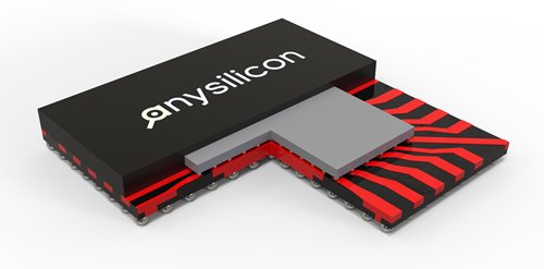
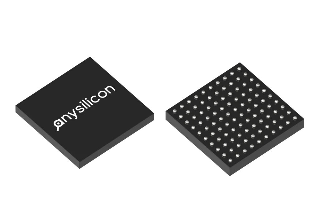
BGA (Ball Grid Array) is a packaging option that is popular for ICs that require a large number of I/O connections.

BGA advantages include low inductance and good heat dissipation options. On the disadvantage side, inspection and fault detection is more difficult, and the cost may be higher compared to other packages such as QFN.
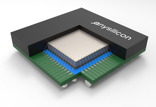
BGA (Ball Grid Array) is a popular IC package type that provides a high level of connectivity and reliability. It features an array of solder balls on the underside of the package, which are used for connecting the IC to the PCB. BGA packages can handle high pin counts and offer excellent thermal performance due to the large number of solder balls that act as conductive pathways for heat dissipation.
QFN (Quad Flat No Lead) is one of the most popular semiconductor packages today due to its low cost, small form factor and good electrical and thermal performance.
The downsides of QFN include low pin count, potential oxidation problems and reliability in long-life, severe environments.
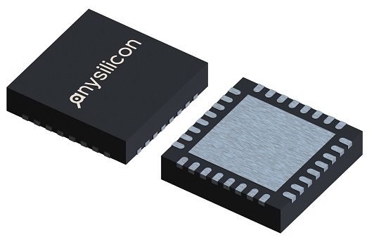
QFN (Quad Flat No-Lead) is another commonly used IC package type. It has a flat bottom with exposed leads on the sides, making it easy to solder onto the PCB. QFN packages offer good thermal performance and a smaller footprint compared to BGA packages, making them suitable for applications where space is limited.
WLCSP (Fan-in Wafer Level CSP) is essentially a bumped die, and therefore offers the smallest possible package size, as it will be the same size as the die.
WLCSP offers reasonably low cost, small size, and good electrical performance but maybe less suitable for high-pin count applications.
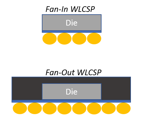
WLCSP (Wafer-Level Chip Scale Package) is a type of package that is directly fabricated on the wafer during the manufacturing process. It offers the smallest form factor and provides excellent electrical performance, as the interconnects are essentially the shortest possible. WLCSP packages are commonly used in mobile devices and other applications where size is a critical factor.
![]()
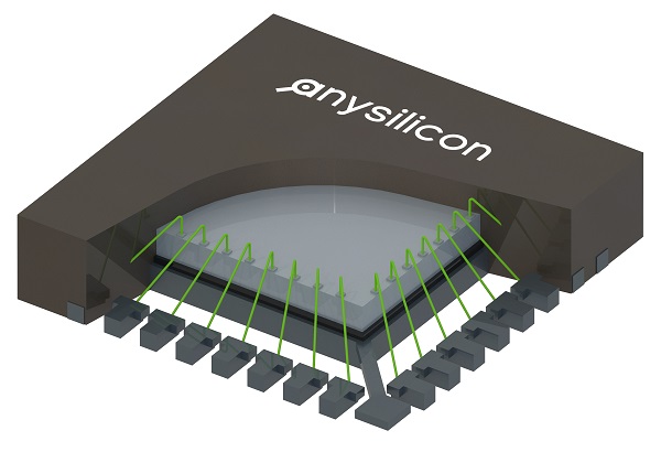
eWLB (Embedded Wafer Level Ball Grid Array) uses an interposer wafer under the original wafer to allow fan-out and more space for interconnect routing. This creates a larger die area and solves interconnect problems of WLCSP.
eWLB is becoming the preferred choice when used with consumer and wireless ASICs.
eWLB (embedded Wafer-Level Ball Grid Array) is a package type that combines the benefits of WLCSP and traditional BGA packages. It offers a compact form factor like WLCSP and excellent electrical performance, while also providing the robustness and reliability of BGA packages. eWLB packages use an embedded wafer-level redistribution layer that allows for a higher pin count and improved electrical connectivity.
There are various types of IC packages available to suit different requirements and applications. Let’s take a closer look at some of the additional commonly used IC package types:
The Dual-in-line Package (DIP) was one of the earliest types of IC packages and is still widely used today, especially for through-hole mounting. It consists of two parallel rows of pins that extend from the body of the package, allowing for easy insertion into a socket or PCB.
DIP packages have the advantage of being relatively easy to handle and solder, making them popular for hobbyist projects and prototyping. However, they have the disadvantage of taking up more space compared to surface-mount packages, limiting their use in applications requiring miniaturization.
SOIC packages are surface-mount packages that have become very popular due to their compact size and versatility. They are available in various sizes and pin counts, making them suitable for a wide range of applications.
SOIC packages have a rectangular body with two or more rows of pins along the sides. They can be soldered directly onto the surface of a PCB, making them more suitable for automated assembly processes. The smaller size of SOIC packages allows for higher-density circuit designs, saving valuable board space.
TSOP packages are a variation of the SOIC package, with a thinner profile. They are commonly used for applications that require a low profile or space-saving design.
TSOP packages have a rectangular body with leads on two sides, making them suitable for surface mounting. They are commonly used in applications such as memory devices, such as RAM and flash memory, where space is limited.
One advantage of TSOP packages is their ability to provide higher pin counts compared to other package types. This allows for more complex and densely packed integrated circuits. However, the smaller size and thinner profile of TSOP packages can make them more challenging to handle and solder, requiring specialized equipment or techniques.
Small-outline (SOIC) packages are another common type of IC package that is widely used in electronic devices. They are similar to SOIC packages but have a slightly different form factor. SOIC packages have a smaller overall height compared to other packages, allowing for more compact circuit designs.
SOIC packages have a rectangular body with leads on two sides, similar to TSOP packages. However, they have a larger body size compared to TSOP packages, which means they can accommodate more pins. This makes them suitable for applications that require a higher pin count, such as microcontrollers or complex integrated circuits.
One advantage of SOIC packages is their compatibility with automated assembly processes. The leads on the package are designed to be easily soldered onto the surface of a PCB, making them suitable for high-volume production.
In addition to their compact size, SOIC packages also provide good electrical performance. The tightly spaced leads minimize parasitic capacitance and inductance, allowing for efficient signal transmission and reduced signal interference.
Another advantage of SOIC packages is their thermal performance. The larger package size allows for better heat dissipation, making them suitable for applications that require higher power dissipation.
Small-outline Package (SOP) is another commonly used IC package in the electronics industry. It is similar to both SOIC and TSOP packages but with a different lead configuration. SOP packages have leads on all four sides of the rectangular body, making them versatile for a variety of applications.
SOP packages are available in different sizes and pin counts, ranging from 8 to 64 pins or more. This makes them suitable for a wide range of integrated circuits, from simple logic gates to complex microcontrollers. The ability to accommodate a larger number of pins allows for more functionality and flexibility in circuit designs.
One advantage of SOP packages is their ease of handling and installation. The leads on all four sides make it easier to place and solder the package onto a PCB, reducing the risk of misalignment. This makes SOP packages suitable for both manual and automated assembly processes.
SOP packages also provide good electrical performance. The closely spaced leads minimize parasitic capacitance and inductance, allowing for efficient signal transmission and reduced signal distortion. This makes SOP packages suitable for high-frequency applications, such as wireless communication devices.
Furthermore, SOP packages offer good thermal performance. The larger package size enables better heat dissipation, which is crucial in applications that generate a lot of heat.
Quad-flat Package (QFP) is a popular IC package that offers a high pin count and compact design. It is commonly used in a wide range of electronic devices, including microcontrollers, memory chips, and digital signal processors.
QFP packages have pins on all four sides, allowing for a higher pin density compared to other IC packages. This makes them suitable for integrated circuits with a large number of I/Os and complex functionality. The compact size of QFP packages also helps in saving space on the PCB, making them ideal for applications where board real estate is limited.
One of the key advantages of QFP packages is their ease of assembly. The leads on all four sides make them suitable for automated assembly processes, reducing manufacturing costs and improving production efficiency. The standardized pin configuration of QFP packages ensures a consistent and reliable connection between the IC and the PCB.
In terms of electrical performance, QFP packages offer excellent signal integrity. The short lead lengths and closely spaced pins minimize parasitic capacitance and inductance, reducing signal distortion and achieving high-speed data transmission. This makes QFP packages ideal for applications that require fast and accurate signal processing, such as in communication systems and consumer electronics.
QFP packages also excel in thermal performance.
Another type of IC package is the Small-outline Transistor (SOT) package. SOT packages are commonly used for discrete components such as transistors and diodes. They are small and compact, making them suitable for applications where space is limited.
SOT packages come in various sizes, with the number of leads ranging from 3 to 6. They have a small footprint on the PCB, which helps in reducing the overall size of the electronic device. This makes SOT packages commonly used in portable electronics, such as smartphones and tablets.
The compact design of SOT packages also contributes to their ease of assembly. They can be easily mounted on the PCB using automated processes, allowing for efficient and cost-effective manufacturing. The standardized pin configuration ensures a reliable connection and simplifies the assembly process.
In terms of electrical performance, SOT packages offer good signal integrity. The short lead length and close proximity of pins help in reducing parasitic capacitance and inductance, minimizing signal distortion and ensuring accurate signal transmission. This makes SOT packages suitable for applications that require high-speed data processing, such as in digital circuits and audio devices.
Your target application is the primary driver dictating your package selection. Is your application a low-cost consumer device or a high-cost industrial ASIC? Will it be running in a hot environment? Will you develop a System on Chip or will your ASIC be a key component within the system?
Such questions will help you decide on the type of packaging – whether you can you use wafer-level or chip-size package, or can standard, more readily available BGA or QFN type packaging be more relevant.
Application performance requirements and the corresponding packaging options can be broadly categorized into three groups:
High-end application requirements are often related to high-speed, high-power chips that have a large number of connections (high pin-out). These devices will require advanced packaging requirements to match the needs of small pad pitch, high-speed signals and decoupling, that can be achieved with the FC-BGA (flip chip BGA), or newer packaging like embedded Wafer Level Ball Grid Array (eWLB).
The Mid-range group typically require packaging that can address thermal enhancements and employ cost-effective plastic packaging technologies – often in the BGA and QFN type approach. At the higher end of this group are chip level and wafer level packaging, suitable for system in package and/or multi-chip module packaging.
The Entry level group includes high-volume applications where cost is the main driver rather than performance. Devices for notebook and mobile applications, for example, will generally require small size wafer level and chip size packaging.
The number and location of input and output connections of any device are key factors to be considered when determining the package requirement. In addition the type of interconnect as in power connections, high speed data inputs and outputs, ground connections and control and monitoring signals need to be clearly identified and related to chip and package layouts.
High pin count. If you’re looking at a very high pin-count, say 1000 pin package, then your best option may be a standard BGA package, which offers such I/O capability as overall package size can go up to 50-60 mm square.
Low pin count. For a low pint count, say 50 pins your choice would probably be a QFN or WLCSP package. However, a WLCSP will have limitations for heat dissipation within the package. In cases where there is heat generation (e.g., fast switching) or need for good signal grounding, then a QFN is the better package choice, due to the ‘built-in’ metal base pad.
Layout. Another parameter is the location of I/Os. If the I/Os are on the periphery around the die, then wire bonding is quick, easy and reliable provided there is enough surface area in the die and package pads for this. If the I/Os are spread across the surface of the chip in different areas, so that wire bonding out from the center of the chip is difficult, then flip chip packaging offers a direct attach approach onto the substrate of the package, which is usually a multi-layer PCB, and there would be no concerns about the die overlapping.
Advances in silicon technology are continually producing chips that are smaller and faster, which means they are also creating more heat. Consequently, thermal management is a key packaging factor for optimizing chip performance.
Heat management ensures the reliability and enduring operation of the chip. For example, interconnections – like the die attach material, wire bonds or Flip Chip balls – are far more reliable if temperatures are kept down. For example, if an ASIC chip is placed on a substrate using epoxy and then the temperatures run too high, the epoxy will soften and possibly melt, allowing the ASIC to physically move, causing the package to become unreliable. Excessive heat may also have a negative effect on RF frequencies and reduce device performance.
Heat management is also a cost factor – depending on the type of device and package selected. Various heat dissipation processes and methods are associated with different package types. A BGA package, for example, can often offer lower cost/improved thermal management solutions within the package because of its size, as it has a larger area available to dissipate the heat. The smaller real-estate chip tends to create a thermal environment that can be more expensive in terms of the thermal management solution, requiring an external heatsink or other cooling options.
BGA (Ball Grid Array) packages have options with both thermal pads, such as conductive vias or inbuilt metal base plates that can enable adequate heat management. Some options of thermally enhanced BGA packages can have a metal cap built onto them that establishes a thermal conduction path between the IC device and the metal cap, which provides good heat dissipation.
QFN (Quad Flat No-Lead) packages are designed such that they have a solid metal die pad as the base of the package, to which the die is bonded. This enables very good heat dissipation from the silicon die through to the PCB.
Die attach materials. Bonding the chip to the substrate with a thermal conductive adhesive like Sliver filled Epoxy, rather than plain epoxy, will help remove the heat. In addition, newer technologies are available like Silver sinter technology – an interconnection method with high operating temperature, high thermal and electrical conductivity. These materials typically work well in QFN packages, but are not as effective in BGA packages, due to the package construction.
Chip size and wafer-level packaging. Thermal management in these packages is primarily done on the back of the chip, or in chip size package, on the exposed top-side of the chip.
RF, wireless and high-speed digital designs have specific requirements that affect package selection. The signal speed and the frequencies can be significantly degraded by the parametric effects of the interconnections within the package.
Wire bond vs. flip chip. In RF devices, key design considerations involve inductance, capacitance and resistance, which are affected by the speed of the signals travelling in and out of the device. These issues also impact package selection, primarily between flip chip and wire bond interconnections. Flip chip will provide better RF Performance and enable reaching higher frequencies with lower inductance. Wire bonds, on the other hand, can add a randomly-variable inductance at each RF input or output at higher frequencies.
Package layout. At RF frequencies, signals travel along the surface rather than in the conductor. Hence, the way in which the package is assembled has an important effect on the device. For example, high-speed amplifier chips, RF transistors, and diodes often cannot be put into a “standard” plastic package, as the encapsulation materials affect the speed in which the chip operates. Consequently, such chips should go into a cavity QFN or BGA package.
High frequency signals (1 GHz and above) are likely to require the layout of the interconnections to have isolated signal paths, known as “ground signal ground” interconnect. Here the requirement of two ground connections for every signal i/o will impact the package size and layout.
Additionally, with high-speed ASICs, the signal levels and timing will be affected by the length of the conductor that they travel along. For example, if you are using a BGA package and you have a longer lead to one point and a shorter lead to the next, you will have timing differences on the signal. This must be overcome by putting more consideration into the initial design of the package substrate to accommodate the high-speed RF devices.
BGA substrate dielectric materials are also a key factor in RF chips. For example, a high-performance liquid polymer substrate, like Rogers laminate, is better suited than the standard FR4 PCB material for use as the substrate for BGA packages used for RF designs.
Specific environmental or mechanical needs tend to determine the type of package required for the application. Consumer products have the simplest requirements (see table below) as the package tends to be driven by cost, rather than environment. Plastic package options are preferred but even here, shock and vibration resistance needs are a limiting factor for the types available.
However, if the application and the system chosen require protection from moisture or chemical effects, as in many medical and aerospace applications, the need for package hermeticity is the driver. In such cases, the only option may be to use a specific type of package, such as a hermetic metal or ceramic package, to protect the ASIC device.
In Automotive applications packages need to withstand levels of temperature, vibration and shock which are now on a level with Defense and Aerospace requirements (See MIL Standards). Nevertheless, since cost is a key driver in Automotive, the industry has improved the performance of standard packages enabling the acceptance of QFN and certain BGA types of parts.
In the space industry, high-speed, low-cost ASIC devices are needed for next generation space capsules and satellites. Here, the applications require packaging that is low-cost and lightweight but can also withstand high G-force, mechanical shock, and pressure. A potential solution may be a plastic package, although these types are not hermetic. The need is driving these applications to look at new ways of sealing the complete systems to overcome the package deficiencies.
The table below provides examples of some environmental requirements in different industries and some potential packaging solutions.
In most cases, the specific application requirements will dictate the package type and form factors. Yet many new applications, such as hand-held devices, next generation ASIC devices with wafer level features such as Through Silicon Vias (TSV’s) may make a package unnecessary. In such cases, a direct die attach/flip chip process will be undertaken.
ASICs often support functional devices such as sensors and LEDs, where the package is not a standard of the type discussed above, but the package, or housing of the electronics must fit into a specific shape and space defined by the application. Typical applications in Automotive, Aerospace and Industry may adopt this approach. For example, the ASIC chip might need to fit into a specific space, such as a power module or into a sensor control system housing.
In other cases, such as when building an automotive module, a System in Package (SiP) may be used, bundling multiple ICs into one overall package along with peripheral devices. Here, custom ceramic package’s such as Pin Grid Arrays or metal can module packages may be used.
Get an indicative packaging cost range, then a detailed breakdown by email.
