

Higher bus speeds and lower power consumption are design criteria for most modern digital electronic products. Packaging solutions that provide higher bus speeds at reduced power per bit ratios require design techniques that shorten the distance between chips (to reduce drive currents) and use wider data buses (with finer line-space traces). Through Silicon Vias (TSVs) solve these challenges but require new test strategies to qualify these designs while keeping quality and cost within design targets.
The IC Test Issue
Electrical testing of TSVs can only be performed after the back-grind and etch processes expose the TSVs – a task that is usually performed at the Outsourced Assembly, and Test (OSAT) supplier. Figure 1 illustrates this dilemma. Therefore, when a TSV interposer wafer leaves the foundry, the quality of the TSVs remains unknown until it is processed at the OSAT.
Within a package, the functions of the TSVs can vary widely. Basically, these connections may be used to carry DC current to power the chip or carry high-speed signals for input /output (I/O) pins or provide low-impedance paths which connect the die to the ground plane. Based on their functions, specific tests need to be performed to verify TSV functionality. Furthermore, TSVs need to undergo characterization tests such as stress and electromigration to quantify their long-term reliability.
Exploring Alternatives
Defects in TSV structures are potentially caused during their manufacture at the foundry or during the TSV “reveal process” at the OSAT. During the fabrication of TSVs, micro-voids, due to quasi-conformal plating, might lead to weak-opens in TSVs, while ineffective removal of the seed layer might lead to shorts between TSVs.
Much effort has been expended in testing the quality of an interposer after active-die or dies attachment. These techniques include Built-In-Self-Test/Diagnosis/Repair (BIST/D/R), Reduced Pad-Count Testing (RPCT), Test Data Compression (TDC), and more. If a problem with a certain path is identified, these approaches rely on redundant resources that can be used to restore device functionality. However, problem identification occurs after an expensive application specific integrated circuit (ASIC) has been attached to the interposer/substrate. If these techniques are used when the first die is attached on a multi-chip module, they can detect problems early in the assembly process. At this point, testing can identify if the problem can be fixed by using an alternate electrical path, apply the fix, and then verify the fix or if no redundancy exists, fail the subassembly before more dies are added, reducing scrap costs.
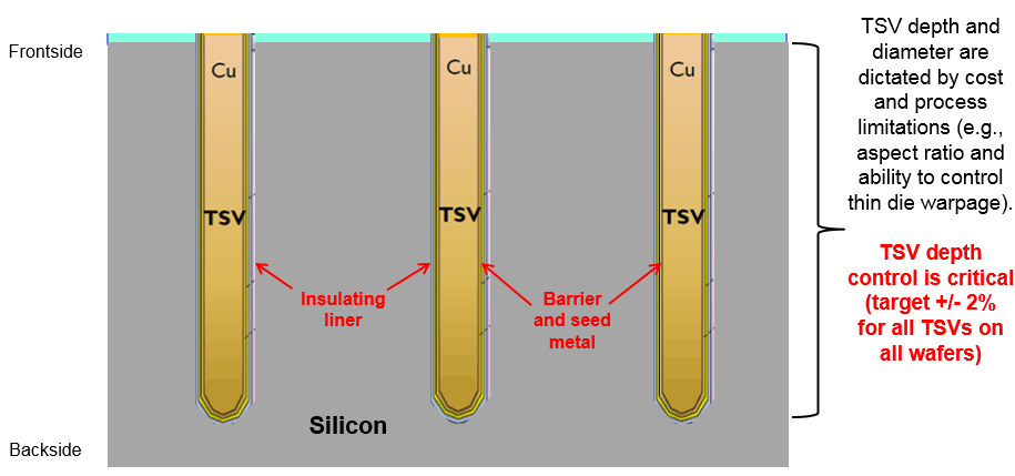
Figure 1: Interposer wafer with TSVs as received from fab.
Often, the ASIC used with the TSV interposer is a large die, which typically is a high-end processor, with about 60% to 70% of the dies per wafer meeting the performance criteria of the final package. Utilizing one of these premium ASICs to identify a fault in the interposer is an expensive option and not the optimal use of a scarce resource – the ASIC.
To achieve the lowest scrap cost, methods of testing the interposer die before it is attached to a substrate should be explored. An easier approach, but at a slight higher cost, would be testing the interposer vias after it is attached to the substrate.
Alternatively, the interposer designer can use multiple redundant vias “n+1”, where “n” represents the number of redundant vias for a single vertical connection. This method works well when there is adequate space under the ASIC, however, as the size of the die shrinks, the number “n” tends to zero i.e., no redundancy, leaving space only for a single via per connection. Furthermore, current trends in the reduction of pad size and pitch might limit the ability to place redundant TSVs for each connection. Therefore, it is necessary to establish robust manufacturing methods for TSVs that result in ultra-high yields.
Case STUDY: TSV supplier qualification
After analyzing potential sources for defects, test techniques (including optical and electrical methods), and test location (foundry or OSAT) alternatives, a project was initiated to confirm the results of the analysis and verify acceptable qualification approaches. As shown in Figure 2, a test vehicle was defined which resembles the final product interposer and allows its use for both interposer vendor qualifications as well as the package-assembly process qualification. This would imply that the test vehicle and the final product would share the same physical size, quantity, and location of the micro bumps/controlled collapse chip connection (C4s). A good practice is to have the test vehicle wired with multiple daisy chain test structures, where each structure is a set of TSVs grouped by their position on the die (e.g. GPU1 NW Corner) with the goal for the daisy chain to flow through every single TSV in that area. Creating regions helps in the failure analysis team to zero-in on the fault area.
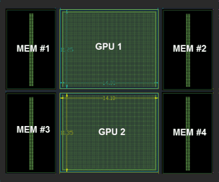
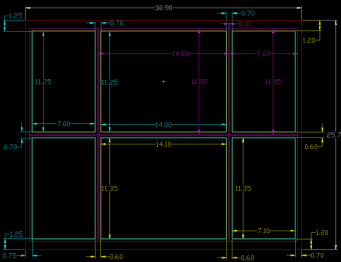
Figure 2: TSV interposer test vehicle.
Interposer Designed for Test
As shown in Figure 2, the end product interposer design was translated into a test vehicle. With a micro bump size within the sub 25-µm range and a C4 size of around 80 µm, the final product accommodated approximately 75,000 micro bumps and about 25,000 C4s.
For versatility, the test structures were designed to break the daisy chains into sub-chains. The electrical path for each sub-chain would be completed by a metal layer on the interposer. Additionally, the sub-chains would be joined to form the full chain using metal layers from the top-die test vehicle, as shown in Figure 3.
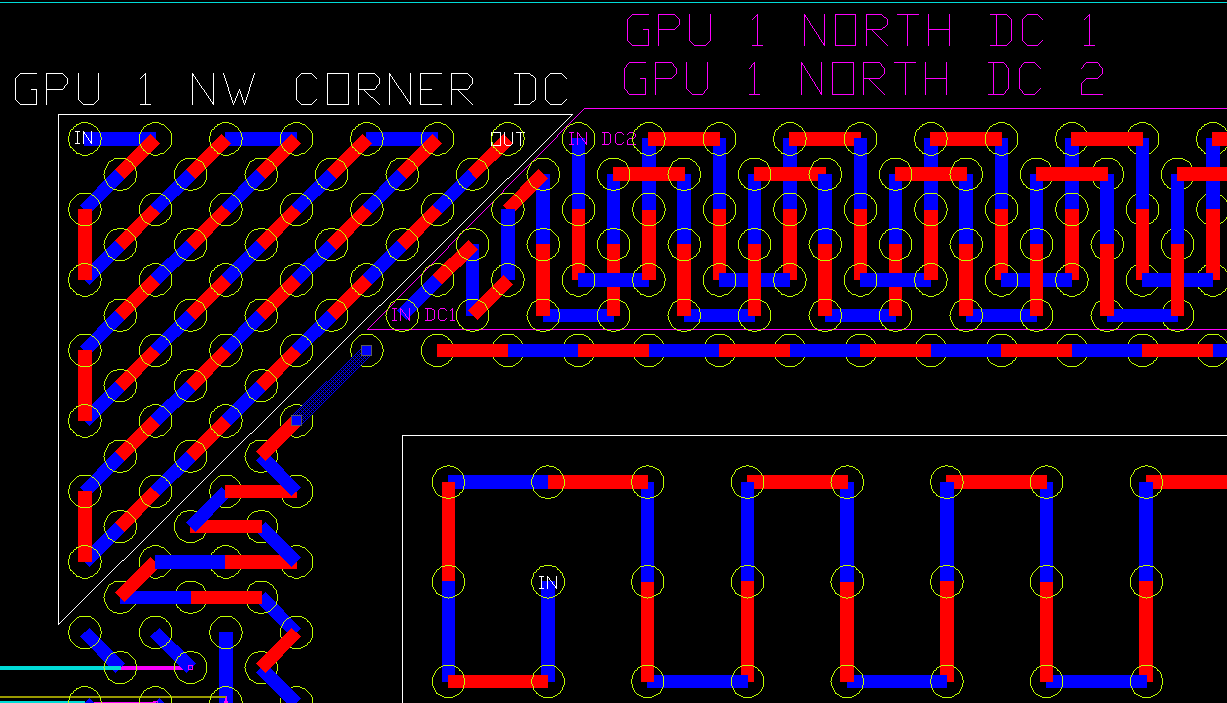
Figure 3: Daisy chain top die (red) and interposer (blue).
Additionally, the test vehicle was used to study the impact of stress and strains which the interposer die will experience when the package is fully assembled (i.e., with top dies attached, under-filled, stiffener ring attached, and the complete assembly over-molded, etc.), therefore, the location of the daisy chains was critical. Daisy chain structures were placed in areas where the large mechanical stress and strain affect the reliability of the TSV structures. Additionally, the test vehicle incorporated strain gauge structures, which was used to measured and monitor stress/strain on the package through the assembly process.
Daisy Chain Resistance Selection
The designer has to choose the resistance values of the daisy chains bearing in mind the metrology. From an equipment perspective, when the number of networks to be measured is below two dozen, a traditional ohmmeter can be used, however, when it exceeds a hundred, the choice of equipment switches to automatic test equipment (ATE) or open-short testers. The metrology ATEs use to test for opens or short is called force current, measure voltage (FIMV). They achieve this by setting the clamp voltage to 3V (adjustable) and forcing a current of 100 µA, then measuring the voltage between the pin under test and ground. The supply and ground pins are connected to ground. A voltage measurement between 0.2V to 0.8V (diode forward voltage) would indicate that the pin under test is connected to the silicon. An open would be indicated by a measurement of clamp voltage and a short (to VDD or GND) by a 0V reading.
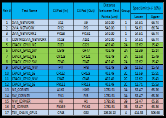
Figure 4: Test list, C4 pads and test limits.
ATE machines complete the measurement in a couple of milliseconds and are not expected to provide an accurate resistance measurement, rather just provide a pass or fail result. Thus it is best for the designer to maintain the daisy chain resistance values between 300 ohms and 3 kilo ohms.
Furthermore, most ATE tester configurations have up to 2500 pins available for test; therefore, the designer must balance the lengths of the daisy chain and the nets to within the tester pin counts.
Vendor Qualification – Test Metrology and Apparatus
One of the key requirements for the evaluation was to provide quick feedback on the quality of the interposer; therefore, it was decided co-locate test with the assembly line, limiting the equipment choice. The prober available on the assembly line was a semi-automatic PA300 with 12-inch wafer capability. The test setup, probe card, and test program had to be simple and intuitive for an operator to use and provide downstream feedback.
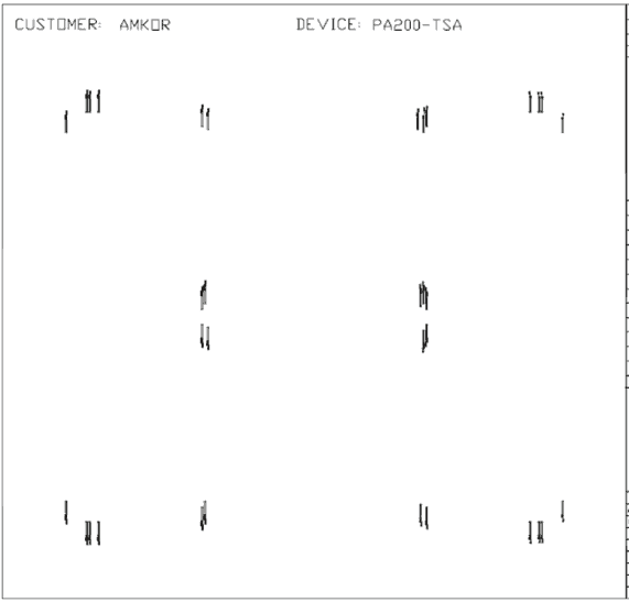
Figure 5: Probe locations for test vehicle.
To limit the size of the experiment, seventeen test structures (Figure 4) were selected, located symmetrically in the four quadrants of the die (Figure 5). A cantilever probe card was used with four-wire capability, with two probes (force+ and sense+) landing on daisy chain input C4 bump, and two (force- and sense-) on the output C4 as seen in Figure 6.
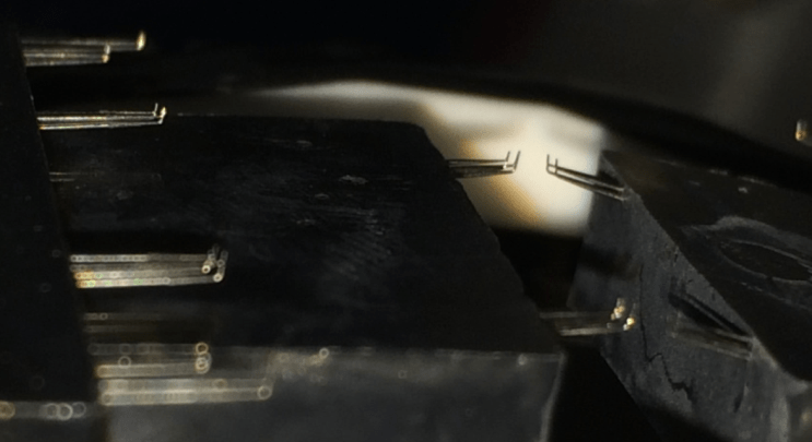
Figure 6: Cantilever probe card – zoomed in.
The test condition was “DC” only – i.e., resistance testing. High-frequency performance was done separately using 50-ohm co-planar waveguide test structures on the interposer and performed using a network analyzer. To avoid the additional, reflow step, the balanced contact force (BCF) was tuned to limit the damage on the C4 during probe, see Figure 7.
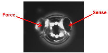
Figure7: Scrub mark overdriven to show force/sense.
Using the interposer design information such as the trace width, thickness, and the daisy chain length, resistances for each daisy chain structure were computed, creating the test specification and the pass-fail limits. The test equipment consisted of four relay boards that switched the four-wire lines from the two Keithley 2400’s source-measure units to two probe transition boards that mapped the measurement point to the probe needles as shown in Figure 8.
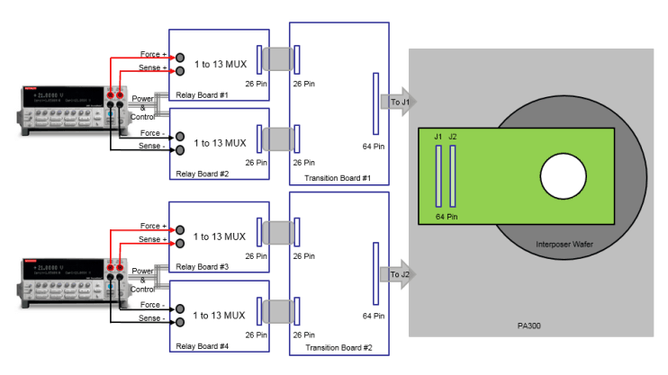
Figure 8: Test setup.
Since a semi-automatic prober was used, the interposer wafers that were mounted on carriers were loaded manually on to the PA300 prober. The optical character recognition (OCR) feature was not available on the prober, so all carrier wafer IDs were manually recorded and later mapped to the interposer ID. Figure 9, shows an interposer wafer mounted on a carrier.
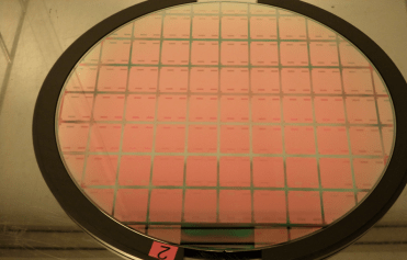
Figure 9: Interposer wafer on carrier.
Test Data Resistance Measurements Interposer Rev# 1
In the first revision of 25 interposer wafers, the test data was collected and the measurement showed consistency across all wafers (Figure 10). Since the test structures chosen were symmetrical (Figure 5), it provided a way to compare the test structure results across the four quadrants of each die and with the wafer as a whole. From the histograms generated, the consistency within the datasets proved that both the measurement metrology and TSV manufacturing techniques were stable. Failures were observed at the outside ring of the interposer wafer (Figure 10). Within the die these failures were not limited to a particular area or test structure, but observed randomly distributed across the test structures.
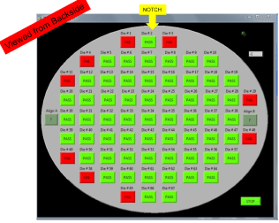
Figure 10: Wafer map and measurement histogram.
An attempt was made to measure the leakage currents in the order of a few femtoamperes (fA) on some of the test structures, but the 6-foot-long cables that connected the transition board to the probe card (Figure 11) proved to have a higher leakage than the 100 fA target measurements.
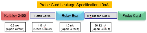
Figure 11: Open-circuit leakage measurements.
This measurement could detect leakages in the order of a few of microamperes, identifying weak shorts. However, since substrates are considered “bad” only when its leakage currents exceeded 100 µA, setting fail criteria for the interposers a couple of orders of magnitude higher than the substrate it attaches to, would result in over rejection of interposer die. As a result, investing in a test setup to measure femtoamperes of leakage did not justify the expense and was found unsuitable for high-volume production.
Test Data Resistance Measurements Interposer Rev# 2
After presenting the first round of measurement data to the interposer supplier, changes were made to the TSV fabrication process and a second revision of interposer wafers were provided to test. The results of the second round of test data showed a huge improvement in the quality of the interposer. In version 1 of the interposers, out of the 28,475 test structures, there were approximately 276 failures. In the second version, for the same number of test structures the failures dropped to 9, a clear indication that process improvements/revisions could improve TSV yield.
TESTING IS OPTIONAL
While electrical test of interposers adds a level of confidence to the quality and connectivity of the die, it also adds cost and consumes real estate. Armed with test data, and mathematical models, we can conclude with high confidence that electrical testing of TSVs are not required after an interposer vendor is qualified and produces high-yielding wafers.
When the test step is eliminated, adding 100% automatic optical inspection (AOI) into the interposer fabrication process prevents blind-assembly builds. Furthermore, the AOI step acts as a process watchdog which can quickly identify manufacturing process drift, sustain yields and provide high-quality interposers without test.
Estimate NRE for test development and an indicative per-unit test cost.
REFERENCE:
[1] Gerard John, “A Practical Approach to Test Through Silicon Vias (TSV),” IWLPC 2016, Oct.18-20, 2016
_____________________________________________________________________________________
This is a guest post by Gerard John, Senior Director Advanced Test, Amkor Technology Inc., Tempe, Arizona, USA,
Gerard.john@amkor.com


