

On Chip Variation (OCV) is an increasing problem that starts at 130nm and its effects are increasing with smaller process nodes. And On-Chip Variation (OCV) is one of them, specifically for Static Timing Analysis.
The first task is to find all possible sources variation, and find out how these can affect a delay of a cell and hence, timing.
In this article I will focus on the various sources of on chip variation:
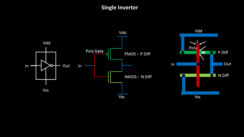
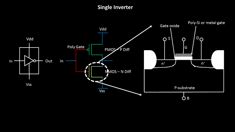
Let’s look into the below layout of an inverter (which also shows the Width (W) and Length (L) parameters of an inverter)
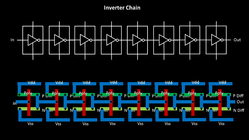
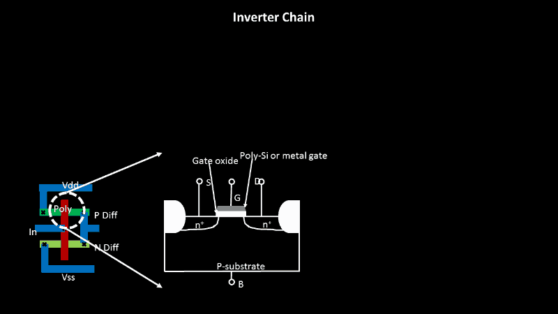
….and, a chain of inverters (this is mostly the case of clock path, be with me for upcoming posts and I will exactly let you know, why OCV is mainly applied on clock paths, 50% should be clear from the term “chain of inverters”)
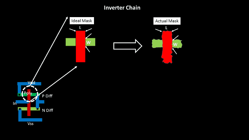
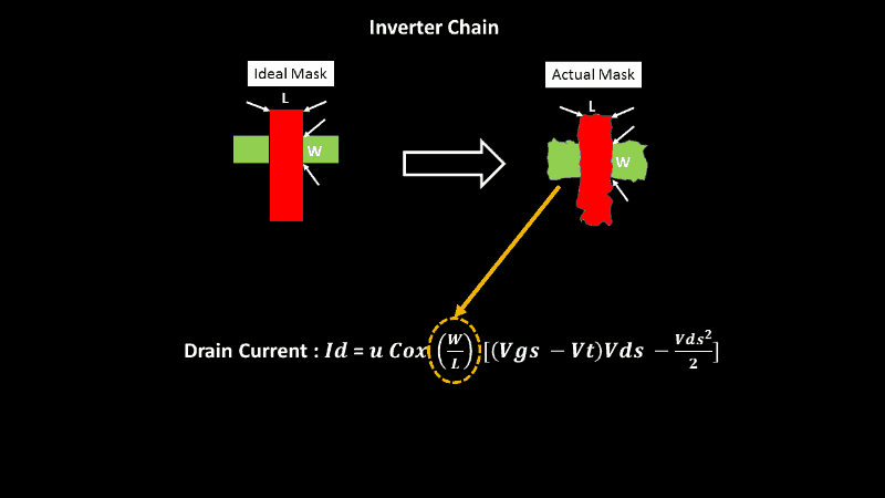
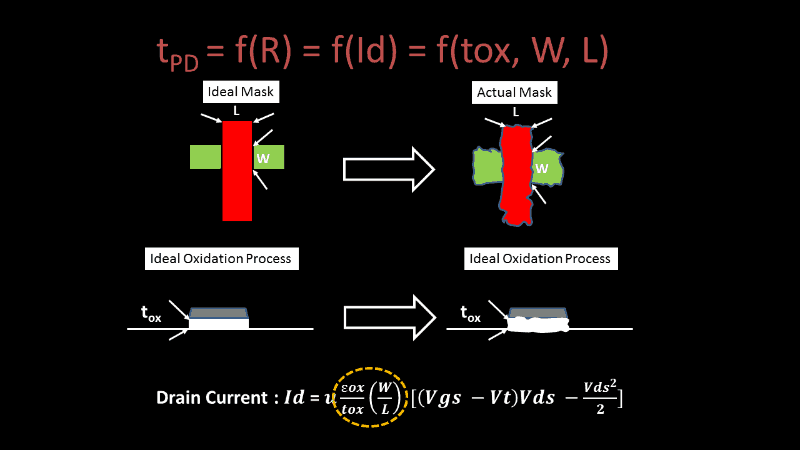
We use photo-lithography fabrication technique to build the inverters on Silicon wafer, and this is a non-ideal process, where the edges will not exactly be straight lines, but there will be disturbances. And why so, because the above technique needs photo-masks which are created using etching, which is again non-ideal. Below is how the ideal mask and real mask look like
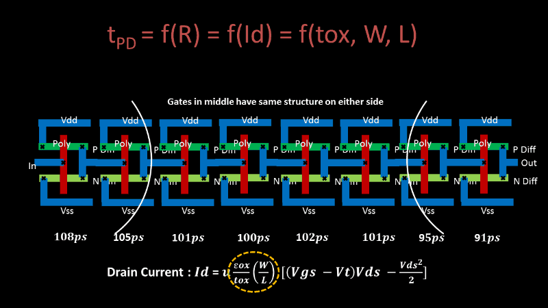
Now these variations on the sides, is also dependent on what logic cell is present on either sides of this inverter, if its surrounded by chain of inverters on either sides, the variation on the sides will be less as the process parameters to build mask for a chain of similar size inverter, is almost the same. But, if the inverters are surrounded by other gates, like flip-flops, then the variation will be more.
With that said, the below inverters in the middle will have a similar and less variations
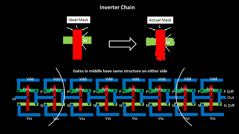
and the inverters on the boundaries will have different and more variations. (observe the difference in actual mask, in above image) And guess what…. this directly impacts the drain current below, as it is proportional to (W/L) ratio
These OCV values he should be used it in STA analysis and see its (+ve or -ve) impact.
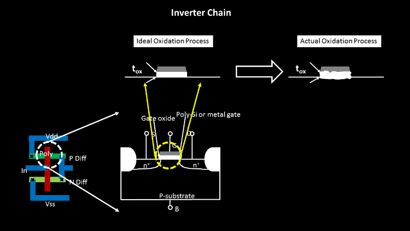
As we were identifying sources of variations, and below is the second one
Let’s go back to the inverter layout and look which part are we talking about. Here, we are talking about gate oxide thickness variation
If we go by ideal fabrication process, below is what you will achieve, a perfectly cubic shape (below is the 2D image, so it looks rectangle) oxide layer, and perfectly deposited metal gate or polysilicon gate
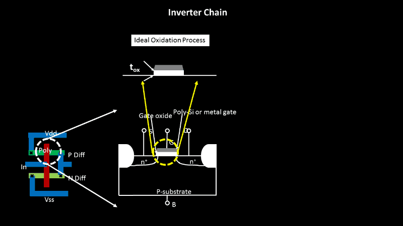
But, if we go by actual oxidation process, it’s very difficult or almost impossible to achieve the above perfect oxide thickness.
Below is what you will actually get
So, what’s wrong having above oxide thickness. Again, it’s the drain current (which is a function of oxide thickness, shown in below image) that will get varied for the complete chain of inverter, especially, the ones on the sides. The variations in middle inverters will still be uniform.
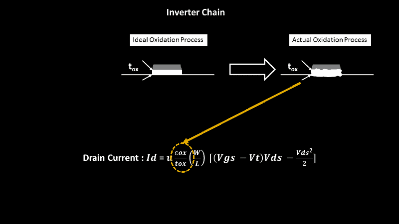
Imagine a chain of, as long as, 40 inverters or buffers…. the variation is HUGE. And this needs to be accounted for, in STA.
So the challenge is, how to we find the range and effectively model it in STA.
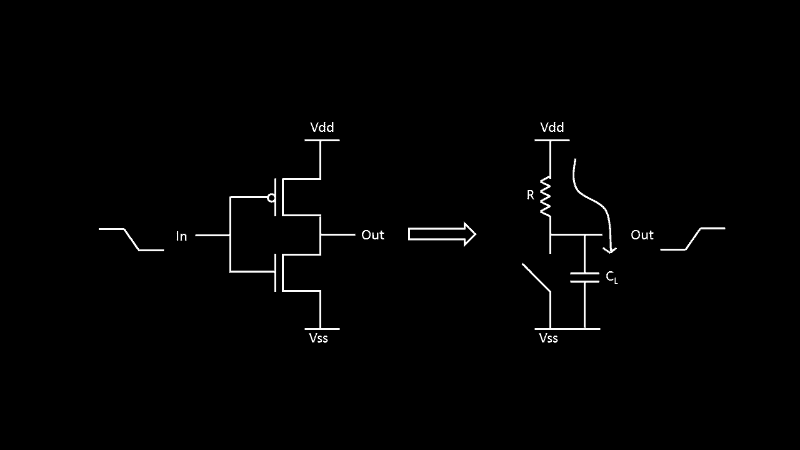
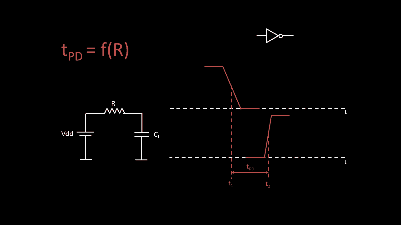
The below image models “low-to-high waveform condition” at input of CMOS inverter, in terms of resistances and capacitances. So, overall, it’s the RC time constant that actually decides the delay of a cell
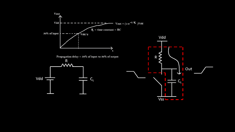
With above, we can safely say, the propagation delay tPD is a function of ‘R’
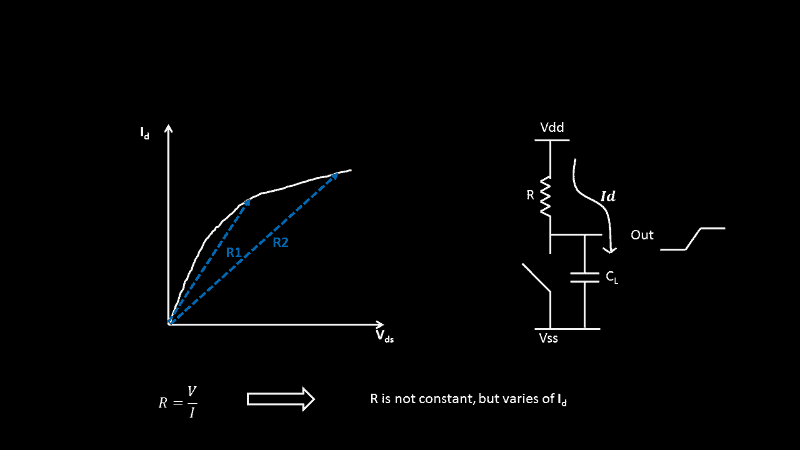
We see variation in drain current ‘Id’ due to variation in ‘W/L’ and ‘oxide thickness’ variations, and above we see, how propagation delay is function of ‘R’. The question is now, what next? If I am, somehow, able to prove, that drain current ‘Id’ strongly depends on ‘R’, then I can directly relate (W/L) and oxide thickness variation to ‘R’, and below images will exactly do that
Hence, every inverter in the below chain, will have delay which is different than the immediate next one, something like below
If we plot a Gaussian Curve with delays on x-axis and no. of inverters on y-axis, it will give us a clue, about the peak variation in inverter delays, the minimum and maximum variation in inverter delays like below
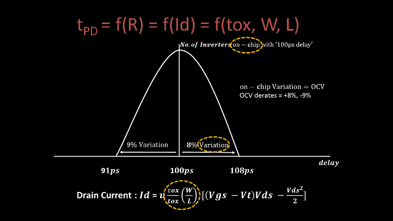
Now, we know the percentage variation in delays of inverter compared to ‘100ps’, because that’s where the inverter delay (with used ‘W/L’ ratio) is expected to be, and most number of inverters on chip with that ‘W/L’ ratio have a delay of 100ps.
OCV variation is +8% and -9% and one of them will be used for launch and other for capture in setup/hold timing calculations. For eg. for setup calculation, the launch clock will have OCV of +8% and capture clock path will have OCV of -9%. That means, if the original clock cell delay is ‘x’ in launch clock, with OCV into account, the same clock cell delay will be (‘x’ + 0.08x). This calculation in setup takes into account the On-Chip Variation, and that’s where the name comes from, as shown in above image.
This is a guest post by Kunal Ghosh with http://www.vlsisystemdesign.com/


