

A key factor in improving memory operations in System on Chips (SoC) is the use of embedded dynamic random-access memory (eDRAM), which means that the DRAM memory is inside the chip. This helps with enhancing the effectiveness and functionality of electronic products by reducing power consumption and offering quicker processing speeds.
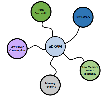
The main goal of eDRAM is to overcome the scalability and performance constraints of conventional DRAM and SRAM technology. eDRAM is embedded directly into the processor chip, providing faster communication between the memory and processing units. It offers a high-bandwidth, low-latency memory solution, which improves data transmission and therefore improving performance of electronic devices such including graphics processing units (GPUs), game consoles, high-end servers, and networking equipment.
Compared to its DRAM and SRAM equivalents, eDRAM technology has the benefit of a smaller footprint in addition to its high speed and low latency characteristics. eDRAM reduces the total size and complexity of the system by taking up less surface space on the device’s motherboard by integrating memory into chipsets.
The evolution of eDRAMs is a fascinating topic that involves the integration of dynamic memory cells with logic circuits on the same chip. eDRAMs offer many benefits, such as high density, low power, and high bandwidth, but also pose many challenges, such as refresh, noise, and yield.
The first eDRAMs were introduced in the late 1980s and early 1990s by IBM, NEC, and Toshiba. They used a trench capacitor structure to store charge in the substrate and a single-transistor access device to connect to the bitline. They were mainly used for video RAM and cache memory in high-end systems. In the mid-1990s, eDRAMs adopted a stacked capacitor structure, which increased the capacitance and reduced the leakage. They also improved the performance and reliability by using sense amplifiers, redundancy, and error correction codes. They were used for graphics memory, network processors, and digital signal processors. In the late 1990s and early 2000s, eDRAMs moved to deep submicron technologies and incorporated advanced features, such as dual-port access, burst mode, and low-voltage operation. They were used for system-on-chip applications, such as mobile phones, PDAs, and digital cameras. In the mid-2000s, eDRAMs became more compatible with logic processes and achieved higher integration and lower cost. They also adopted new architectures, such as macro and array partitioning, hierarchical wordline and bitline, and differential sensing. They were used for high-performance processors, such as IBM’s POWER7, Intel’s Haswell, and many game consoles, such as PlayStation 2, Xbox 360, and Wii U 23. In the late 2000s and 2010s, eDRAMs explored new materials and structures, such as metal-insulator-metal capacitors, silicon-on-insulator substrates, and three-dimensional stacking. They also improved the scalability and variability by using novel techniques, such as assist circuits, adaptive refresh, and self-repair. They were used for emerging applications, such as artificial intelligence, neuromorphic computing, and quantum computing.
As can be seen, eDRAMs have evolved significantly over the past three decades and have become more than just a memory. They have enabled new levels of performance, functionality, and efficiency in various systems and applications.
A type of random-access memory that is fully incorporated into the application-specific integrated circuit (ASIC) is called embedded dynamic random access memory (eDRAM). This integration leads to better performance and lower power consumption in high-speed computing applications. Standard DRAM is significantly less expensive than this technology. However, because it is built within the IC itself, it has a significant advantage over regular DRAM in terms of speed, power needs, and efficiency.
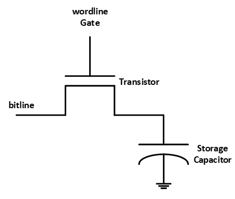
The basic operation of DRAM is as follows:
To write a bit of data, the transistor charges or discharges the capacitor, depending on whether the bit is a ‘1’ or a ‘0’. The wordline and bitline, which are horizontal and vertical lines that link the memory cells, are used for charging and discharging.
§ To read a bit of data, the wordline gets high, and the transistor links the capacitor to the bitline. The charge on the capacitor is then sensed by a circuit known as a sense amplifier, which outputs the corresponding logic level. Because reading from the bitline causes the charge to flow out of the capacitor, the value received must be written back to the capacitor to preserve the data.
§ The capacitors in DRAM leak charge over time, so they must be refreshed periodically to maintain the data stored in memory. Refreshing works just like a read-and-write operation, but it is done for all the memory cells at regular intervals. This is where DRAM gets the “dynamic” name from, as the charge on a DRAM cell is dynamically refreshed every so often.
One of the eDRAM applications is to accelerate data processing for machine learning (ML) tasks, such as deep neural networks (DNNs), which requires massive amounts of data movement from off-chip memory to on-chip processing cores, causing a bottleneck in terms of latency and energy consumption. To overcome this challenge, eDRAM can be used to implement compute-in-memory (CIM) designs, performing analog DNN computations within the memory array, along with peripheral mixed-signal circuits. CIM designs can reduce the data movement and increase the parallelism and efficiency of DNN processing. eDRAM can also enable reconfigurable and adaptive CIM designs, which can adjust the memory size and the computation mode according to the layer and kernel requirements of different DNN models.
Another application of eDRAM is to enable processing-in-memory (PIM) for intelligent Internet of Things (IoT) sensor nodes. IoT sensor nodes often have limited power and computational resources, which limit their ability to perform complex data processing and analysis. Thus, eDRAM can be used to implement PIM designs, which perform data processing within the memory cells, using the charge sharing and sensing operations of eDRAM. PIM designs reduce power consumption and improve the performance of IoT sensor nodes. Moreover, eDRAM enables pseudo-static PIM designs, which can extend the retention time of the memory cells and eliminate the need for refresh, thus improving the area and power efficiency of PIM.
The application of eDRAM in edge computing is to enhance the signal processing capabilities for on-edge applications, such as image and video processing, speech recognition, and natural language processing. eDRAM can be used to implement in-embedded-DRAM-compute designs, performing arithmetic and logical operations within the memory cells using the charge sharing and sensing operations of eDRAM. In-embedded-DRAM-compute designs improve the throughput and energy efficiency of signal processing by reducing the number of pre-charge and activate cycles and enabling pipelining of the continuously arriving digitized signal. In addition, eDRAM enables novel performance-efficient in-embedded-DRAM-compute designs, which employ a bit-serial computation that targets 3x throughput efficiency by arranging the operand bits in an interleaved manner.
The eDRAM applications in wireless communication systems are again to improve performance, power consumption and size. The various functions within wireless systems require large amounts of data movement and computation, which can be optimized using eDRAM as a local memory or a cache. eDRAM can also reduce the latency and energy consumption of data access, as well as the area and power consumption of the memory array. This is a great benefit for battery operated products.
eDRAMs are a type of memory technology that combines DRAM and SRAM technologies. eDRAM has many advantages over both types of memory, including lower power consumption, higher density, and faster speed. One of the major advantages of eDRAM is that it can be installed on the same chip as the processor, reducing the latency and bandwidth limitations of off-chip memory This can enable data-intensive applications such as graphics, video and smart they have been used for things. Another advantage of eDRAM is the use of a simpler and lighter cell architecture than SRAM, reducing space and memory costs. eDRAMs are also capable of lower leakage currents than SRAM, reducing power consumption in memory. eDRAMs are widely used in devices, such as game consoles, laptops and servers.
There are some significant challenges in eDRAM implementation that require further research and development to overcome. eDRAMs are a promising memory technology that can lead to high-performance and simple system design for a variety of applications. eDRAMs store data as electrical energy, which can degrade over time due to various factors such as temperature, configuration changes and noise. Therefore, periodic refresh operations are required to maintain data integrity, consume power and bandwidth. The refresh rate depends on the storage cell configuration, technology node, and operating conditions. Therefore, optimizing the refresh rate for different situations is a big challenge for eDRAM. In addition, eDRAMs use different bitcells, such as 1T-1C, 2T-2C, and gain-cells, which take various trade-offs between area, performance, and reliability For example, 1T-1C bitcells require a different step used to produce high-density capacitors, . While gain-cell bitcells can be used with standard CMOS transistors but have lower storage capacitance and higher leakage current Selecting the optimal bitcell design for a given application and technology is another challenge for eDRAMs. As mentioned, eDRAMs can be integrated on the same chip as the processor, reducing the latency and bandwidth limitations of off-chip memory. But this also introduces some architectural challenges, such as how to allocate memory space, manage the cache hierarchy, and deal with consistency and stability issues Besides, eDRAMs can also benefit from architectural flexibility, such as sub-banking, voltage scaling, and faults.
Intel and IBM have used eDRAM for a variety of applications, such as graphics, video, and artificial intelligence. However, eDRAM also faces some challenges, such as data storage, bitcell design, and memory architecture. Therefore, the future trends in eDRAM development could include the following factors.
As the demand for high performance and low power systems increases, eDRAM may need to scale to smaller nodes such as 10nm, 7nm, or even 5nm. This may require new materials, processes, and designs to achieve more robust and less slippery eDRAM cells. For example, Intel used FinFETs and MIM capacitors for 22nm eDRAM, while IBM used SOI and trench capacitors for 45nm eDRAM12. In the future, eDRAM may require other techniques such as nanowires, nanosheets, or 3D stacking. eDRAM has been used primarily for image and video applications, where it can provide high bandwidth and low latency for large amounts of data. But eDRAM can also be useful in other areas, such as artificial intelligence, where it can speed up computation and communication in neural networks e.g., eDRAM can be used as a buffer, cache, or scratchpad memory for AI accelerators, like GPUs, . TPUs, or FPGAs. eDRAM can also be used as synaptic or neuronal memory for neuromorphic computing, where it can mimic the learning and evolution of biological neurons. In addition, eDRAM can improve the performance and reliability of systems by reducing memory access latency and power consumption. However, eDRAM must also overcome certain issues, such as refresh rate, error rate, and temperature sensitivity.
Therefore, eDRAM may adopt some techniques, such as sub-banking, voltage scaling, and error correction codes, to optimize the refresh rate and reduce the power and area overhead. eDRAM may also use some methods, such as thermal management, adaptive control, and fault tolerance, to enhance the reliability and robustness of eDRAM under different operating conditions.
In summary, eDRAM has a bright future ahead of it that will probably improve efficiency and performance in a variety of computer applications. Higher densities and increased power efficiency are anticipated as a result of eDRAM’s integration with cutting-edge manufacturing technologies, which will be in line with the expanding needs of contemporary electronic gadgets. eDRAM ability to accommodate a wide range of processing requirements is demonstrated by its incorporation into heterogeneous system designs and its possible uses in artificial intelligence and machine learning. With more and more jobs requiring a lot of memory, eDRAM speed and density make it a good option for maximizing data transfer and storage.
In order to meet the growing need for battery-powered gadgets and environmentally friendly computing solutions, efforts to increase power efficiency will probably spur the development of more energy-efficient eDRAM systems. In order to satisfy the changing demands of complex computer systems, eDRAM’s overall efficiency may be further enhanced by advances in materials science and advanced memory management techniques. Current trends indicate that eDRAM will continue to be essential in determining the efficiency and performance of next-generation electronic devices and computer systems, even if the precise course of its development will rely on continued research and technical advancements.


